- 您现在的位置:买卖IC网 > PDF目录10502 > MAX11644EUA+ (Maxim Integrated Products)IC ADC 12BIT I2C/SRL 1CH 8UMAX PDF资料下载
参数资料
| 型号: | MAX11644EUA+ |
| 厂商: | Maxim Integrated Products |
| 文件页数: | 4/22页 |
| 文件大小: | 0K |
| 描述: | IC ADC 12BIT I2C/SRL 1CH 8UMAX |
| 产品培训模块: | Lead (SnPb) Finish for COTS Obsolescence Mitigation Program |
| 标准包装: | 50 |
| 位数: | 12 |
| 采样率(每秒): | 94.4k |
| 数据接口: | I²C,串行 |
| 转换器数目: | 1 |
| 功率耗散(最大): | 362mW |
| 电压电源: | 单电源 |
| 工作温度: | -40°C ~ 85°C |
| 安装类型: | 表面贴装 |
| 封装/外壳: | 8-TSSOP,8-MSOP(0.118",3.00mm 宽) |
| 供应商设备封装: | 8-uMAX |
| 包装: | 管件 |
| 输入数目和类型: | 2 个单端,单极;2 个单端,双极;1 个差分,单极;1 个差分,双极 |
MAX11644/MAX11645
Low-Power, 1-/2-Channel, I2C, 12-Bit ADCs
in Ultra-Tiny 1.9mm x 2.2mm Package
12
______________________________________________________________________________________
Analog Input Range and Protection
Internal protection diodes clamp the analog input to VDD
and GND. These diodes allow the analog inputs to swing
from (GND - 0.3V) to (VDD + 0.3V) without causing dam-
age to the device. For accurate conversions, the inputs
must not go more than 50mV below GND or above VDD.
Single-Ended/Differential Input
The SGL/DIF of the configuration byte configures the
MAX11644/MAX11645 analog-input circuitry for single-
ended or differential inputs (Table 2). In single-ended
mode (SGL/DIF = 1), the digital conversion results are
the difference between the analog input selected by
CS[0] and GND (Table 3). In differential mode (SGL/
DIF = 0), the digital conversion results are the differ-
ence between the + and the - analog inputs selected
by CS[0] (Table 4).
Unipolar/Bipolar
When operating in differential mode, the BIP/UNI bit of
the set-up byte (Table 1) selects unipolar or bipolar
operation. Unipolar mode sets the differential input
range from 0 to VREF. A negative differential analog
input in unipolar mode causes the digital output code
to be zero. Selecting bipolar mode sets the differential
input range to ±VREF/2. The digital output code is bina-
ry in unipolar mode and two’s complement in bipolar
mode. See the
Transfer Functions section.
In single-ended mode, the MAX11644/MAX11645
always operate in unipolar mode irrespective of
BIP/UNI. The analog inputs are internally referenced to
GND with a full-scale input range from 0 to VREF.
2-Wire Digital Interface
The MAX11644/MAX11645 feature a 2-wire interface
consisting of a serial-data line (SDA) and serial-clock
line (SCL). SDA and SCL facilitate bidirectional commu-
nication between the MAX11644/MAX11645 and the
master at rates up to 1.7MHz. The MAX11644/
MAX11645 are slaves that transfer and receive data.
The master (typically a microcontroller) initiates data
transfer on the bus and generates the SCL signal to
permit that transfer.
SDA and SCL must be pulled high. This is typically done
with pullup resistors (750
Ω or greater) (see the Typical
Operating Circuit). Series resistors (RS) are optional. They
protect the input architecture of the MAX11644/
MAX11645 from high voltage spikes on the bus lines and
minimize crosstalk and undershoot of the bus signals.
Bit Transfer
One data bit is transferred during each SCL clock
cycle. A minimum of 18 clock cycles are required to
transfer the data in or out of the MAX11644/MAX11645.
The data on SDA must remain stable during the high
period of the SCL clock pulse. Changes in SDA while
SCL is stable are considered control signals (see the
START and STOP Conditions section). Both SDA and
SCL remain high when the bus is not busy.
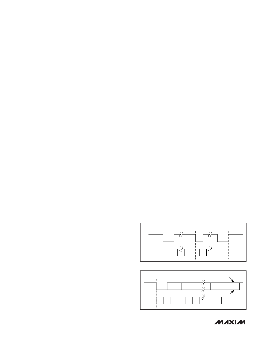
START and STOP Conditions
The master initiates a transmission with a START (S)
condition, a high-to-low transition on SDA while SCL is
high. The master terminates a transmission with a STOP
(P) condition, a low-to-high transition on SDA while SCL
is high (Figure 5). A repeated START (Sr) condition
can be used in place of a STOP condition to leave the
bus active and the interface mode unchanged (see the
HS Mode section).
Acknowledge Bits
Data transfers are acknowledged with an acknowledge
bit (A) or a not-acknowledge bit (A). Both the master
and the MAX11644/MAX11645 (slave) generate
acknowledge bits. To generate an acknowledge, the
receiving device must pull SDA low before the rising
edge of the acknowledge-related clock pulse (ninth
pulse) and keep it low during the high period of the
clock pulse (Figure 6). To generate a not-acknowledge,
the receiver allows SDA to be pulled high before the
rising edge of the acknowledge-related clock pulse
and leaves SDA high during the high period of the
clock pulse. Monitoring the acknowledge bits allows for
detection of unsuccessful data transfers. An unsuc-
cessful data transfer happens if a receiving device is
busy or if a system fault has occurred. In the event of
an unsuccessful data transfer, the bus master should
reattempt communication at a later time.
SCL
SDA
SP
Sr
Figure 5. START and STOP Conditions
SCL
SDA
S
NOT-ACKNOWLEDGE
ACKNOWLEDGE
12
8
9
Figure 6. Acknowledge Bits
相关PDF资料 |
PDF描述 |
|---|---|
| VI-B0W-MX-F4 | CONVERTER MOD DC/DC 5.5V 75W |
| VI-B0W-MX-F3 | CONVERTER MOD DC/DC 5.5V 75W |
| MS3101A18-11P | CONN RCPT 5POS FREE HNG W/PINS |
| VI-B0W-MX-F1 | CONVERTER MOD DC/DC 5.5V 75W |
| VI-B0V-MX-F3 | CONVERTER MOD DC/DC 5.8V 75W |
相关代理商/技术参数 |
参数描述 |
|---|---|
| MAX11644EUA+ | 功能描述:模数转换器 - ADC 12-Bit 2Ch 94.4ksps 5.5V Precision ADC RoHS:否 制造商:Texas Instruments 通道数量:2 结构:Sigma-Delta 转换速率:125 SPs to 8 KSPs 分辨率:24 bit 输入类型:Differential 信噪比:107 dB 接口类型:SPI 工作电源电压:1.7 V to 3.6 V, 2.7 V to 5.25 V 最大工作温度:+ 85 C 安装风格:SMD/SMT 封装 / 箱体:VQFN-32 |
| MAX11644EUA+T | 功能描述:模数转换器 - ADC 12-Bit 2Ch 94.4ksps 5.5V Precision ADC RoHS:否 制造商:Texas Instruments 通道数量:2 结构:Sigma-Delta 转换速率:125 SPs to 8 KSPs 分辨率:24 bit 输入类型:Differential 信噪比:107 dB 接口类型:SPI 工作电源电压:1.7 V to 3.6 V, 2.7 V to 5.25 V 最大工作温度:+ 85 C 安装风格:SMD/SMT 封装 / 箱体:VQFN-32 |
| MAX11645EUA+ | 功能描述:模数转换器 - ADC 12-Bit 2Ch 94.4ksps 3.6V Precision ADC RoHS:否 制造商:Texas Instruments 通道数量:2 结构:Sigma-Delta 转换速率:125 SPs to 8 KSPs 分辨率:24 bit 输入类型:Differential 信噪比:107 dB 接口类型:SPI 工作电源电压:1.7 V to 3.6 V, 2.7 V to 5.25 V 最大工作温度:+ 85 C 安装风格:SMD/SMT 封装 / 箱体:VQFN-32 |
| MAX11645EUA+T | 功能描述:模数转换器 - ADC 12-Bit 2Ch 94.4ksps 3.6V Precision ADC RoHS:否 制造商:Texas Instruments 通道数量:2 结构:Sigma-Delta 转换速率:125 SPs to 8 KSPs 分辨率:24 bit 输入类型:Differential 信噪比:107 dB 接口类型:SPI 工作电源电压:1.7 V to 3.6 V, 2.7 V to 5.25 V 最大工作温度:+ 85 C 安装风格:SMD/SMT 封装 / 箱体:VQFN-32 |
| MAX11645EWC+ | 制造商:Maxim Integrated Products 功能描述: |
发布紧急采购,3分钟左右您将得到回复。