- 您现在的位置:买卖IC网 > PDF目录9899 > MAX1167CCEE+ (Maxim Integrated Products)IC ADC 16BIT 200KSPS 16-QSOP PDF资料下载
参数资料
| 型号: | MAX1167CCEE+ |
| 厂商: | Maxim Integrated Products |
| 文件页数: | 27/30页 |
| 文件大小: | 0K |
| 描述: | IC ADC 16BIT 200KSPS 16-QSOP |
| 产品培训模块: | Lead (SnPb) Finish for COTS Obsolescence Mitigation Program |
| 标准包装: | 100 |
| 位数: | 16 |
| 采样率(每秒): | 200k |
| 数据接口: | MICROWIRE?,QSPI?,串行,SPI? |
| 转换器数目: | 1 |
| 功率耗散(最大): | 667mW |
| 电压电源: | 模拟和数字 |
| 工作温度: | 0°C ~ 70°C |
| 安装类型: | 表面贴装 |
| 封装/外壳: | 16-SSOP(0.154",3.90mm 宽) |
| 供应商设备封装: | 16-QSOP |
| 包装: | 管件 |
| 输入数目和类型: | 8 个单端,双极 |
第1页第2页第3页第4页第5页第6页第7页第8页第9页第10页第11页第12页第13页第14页第15页第16页第17页第18页第19页第20页第21页第22页第23页第24页第25页第26页当前第27页第28页第29页第30页
MAX1167/MAX1168
Multichannel, 16-Bit, 200ksps Analog-to-Digital
Converters
6
_______________________________________________________________________________________
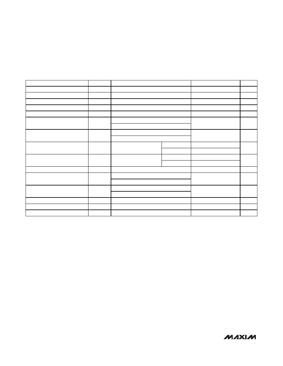
TIMING CHARACTERISTICS (Figures 1, 2, 8, and 16)
(AVDD = +4.75V to +5.25V, DVDD = +2.7V to +5.25V, fSCLK = 4.8MHz external clock (50% duty cycle), 24 clocks/conversion
(200ksps), external VREF = +4.096V, TA = TMIN to TMAX, unless otherwise noted. Typical values are at TA = +25°C.)
PARAMETER
SYMBOL
CONDITIONS
MIN
TYP
MAX
UNITS
Acquisition Time
tACQ
External clock (Note 6)
729
ns
SCLK to DOUT Valid
tDO
CDOUT = 30pF
100
ns
CS Fall to DOUT Enable
tDV
CDOUT = 30pF
100
ns
CS Rise to DOUT Disable
tTR
CDOUT = 30pF
80
ns
CS Pulse Width
tCSW
100
ns
SCLK rise
CS to SCLK Setup
tCSS
SCLK fall (DSP)
100
ns
SCLK rise
CS to SCLK Hold
tCSH
SCLK fall (DSP)
0ns
Conversion
93
SCLK High Pulse Width
tCH
Duty cycle 45% to 55%
Data transfer
93
ns
Conversion
93
SCLK Low Pulse Width
tCL
Duty cycle 45% to 55%
Data transfer
93
ns
SCLK Period
tCP
209
ns
SCLK rise
DIN to SCLK Setup
tDS
SCLK fall (DSP)
100
ns
SCLK rise
DIN to SCLK Hold
tDH
SCLK fall (DSP)
0ns
CS Falling to DSPR Rising
tDF
100
ns
DSPR to SCLK Falling Setup
tFSS
100
ns
DSPR to SCLK Falling Hold
tFSH
0ns
Note 1:
AVDD = DVDD = +5.0V.
Note 2:
Relative accuracy is the deviation of the analog value at any code from its theoretical value after full-scale range has been
calibrated.
Note 3:
Offset and reference errors nulled.
Note 4:
DC voltage applied to on channel, and a full-scale 1kHz sine wave applied to off channels.
Note 5:
Conversion time is measured from the rising edge of the 8th external SCLK pulse to EOC transition minus tACQ in 8-bit
data-transfer mode.
Note 6:
See Figures 10 and 17.
Note 7:
fSCLK = 4.8MHz, fINTCLK = 4.0MHz. Sample rate is calculated with the formula fs = n1 (n2 / fSCLK + n3 / fINTCLK)-1 where:
n1 = number of scans, n2 = number of SCLK cycles, and n3 = number of internal clock cycles (see Figures 11–14).
Note 8:
Guaranteed by design; not production tested.
Note 9:
Internal reference and buffer are left on between conversions.
Note 10: Defined as the change in the positive full scale caused by a ±5% variation in the nominal supply voltage.
相关PDF资料 |
PDF描述 |
|---|---|
| MAX187BCWE+T | IC ADC 12BIT SERIAL LP 16SOIC |
| IDT72V2105L10PF8 | IC FIFO SUPERSYNCII 10NS 64-TQFP |
| MAX1499ECJ+T | IC ADC 3 1/2DIG W/LED DVR 32TQFP |
| MS27472E18F28S | CONN RCPT 28POS WALL MT W/SCKT |
| ISL32272EFBZ | IC XMITTER ESD RS422 LP 16-SOIC |
相关代理商/技术参数 |
参数描述 |
|---|---|
| MAX1167CCEE+ | 功能描述:模数转换器 - ADC Integrated Circuits (ICs) Analog to Digital Converters - IC ADC 16BIT 200KSPS 16-QSOP RoHS:否 制造商:Texas Instruments 通道数量:2 结构:Sigma-Delta 转换速率:125 SPs to 8 KSPs 分辨率:24 bit 输入类型:Differential 信噪比:107 dB 接口类型:SPI 工作电源电压:1.7 V to 3.6 V, 2.7 V to 5.25 V 最大工作温度:+ 85 C 安装风格:SMD/SMT 封装 / 箱体:VQFN-32 |
| MAX1167CCEE+T | 功能描述:模数转换器 - ADC RoHS:否 制造商:Texas Instruments 通道数量:2 结构:Sigma-Delta 转换速率:125 SPs to 8 KSPs 分辨率:24 bit 输入类型:Differential 信噪比:107 dB 接口类型:SPI 工作电源电压:1.7 V to 3.6 V, 2.7 V to 5.25 V 最大工作温度:+ 85 C 安装风格:SMD/SMT 封装 / 箱体:VQFN-32 |
| MAX1167CCEE-T | 功能描述:模数转换器 - ADC RoHS:否 制造商:Texas Instruments 通道数量:2 结构:Sigma-Delta 转换速率:125 SPs to 8 KSPs 分辨率:24 bit 输入类型:Differential 信噪比:107 dB 接口类型:SPI 工作电源电压:1.7 V to 3.6 V, 2.7 V to 5.25 V 最大工作温度:+ 85 C 安装风格:SMD/SMT 封装 / 箱体:VQFN-32 |
| MAX1167CEEE | 功能描述:模数转换器 - ADC RoHS:否 制造商:Texas Instruments 通道数量:2 结构:Sigma-Delta 转换速率:125 SPs to 8 KSPs 分辨率:24 bit 输入类型:Differential 信噪比:107 dB 接口类型:SPI 工作电源电压:1.7 V to 3.6 V, 2.7 V to 5.25 V 最大工作温度:+ 85 C 安装风格:SMD/SMT 封装 / 箱体:VQFN-32 |
| MAX1167CEEE+ | 功能描述:模数转换器 - ADC RoHS:否 制造商:Texas Instruments 通道数量:2 结构:Sigma-Delta 转换速率:125 SPs to 8 KSPs 分辨率:24 bit 输入类型:Differential 信噪比:107 dB 接口类型:SPI 工作电源电压:1.7 V to 3.6 V, 2.7 V to 5.25 V 最大工作温度:+ 85 C 安装风格:SMD/SMT 封装 / 箱体:VQFN-32 |
发布紧急采购,3分钟左右您将得到回复。