- 您现在的位置:买卖IC网 > PDF目录9933 > MAX1185ECM/V+ (Maxim Integrated Products)IC ADC 10BIT 20MSPS DL LP 48TQFP PDF资料下载
参数资料
| 型号: | MAX1185ECM/V+ |
| 厂商: | Maxim Integrated Products |
| 文件页数: | 2/21页 |
| 文件大小: | 0K |
| 描述: | IC ADC 10BIT 20MSPS DL LP 48TQFP |
| 产品培训模块: | Lead (SnPb) Finish for COTS Obsolescence Mitigation Program |
| 标准包装: | 250 |
| 位数: | 10 |
| 采样率(每秒): | 20M |
| 转换器数目: | 2 |
| 功率耗散(最大): | 2.43W |
| 电压电源: | 单电源 |
| 工作温度: | -40°C ~ 85°C |
| 安装类型: | 表面贴装 |
| 封装/外壳: | 48-TQFP 裸露焊盘 |
| 供应商设备封装: | 48-TQFP 裸露焊盘(7x7) |
| 包装: | 托盘 |
| 输入数目和类型: | 4 个单端,单极;4 个单端,双极;2 个差分,单极;2 个差分,双极 |
Detailed Description
The MAX1185 uses a nine-stage, fully-differential,
pipelined architecture (Figure 1) that allows for high-
speed conversion while minimizing power consumption.
Samples taken at the inputs move progressively through
the pipeline stages every half-clock cycle. Including the
delay through the output latch, the total clock-cycle
latency is five clock cycles.
1.5-bit (2-comparator) flash ADCs convert the held input
voltages into a digital code. The digital-to-analog con-
verters (DACs) convert the digitized results back into
analog voltages, which are then subtracted from the
original held input signals. The resulting error signals
are then multiplied by two and the residues are passed
along to the next pipeline stages, where the process is
repeated until the signals have been processed by all
nine stages. Digital error correction compensates for
ADC comparator offsets in each of these pipeline
stages and ensures no missing codes.
Both input channels are sampled on the rising edge of
the clock and the resulting data is multiplexed at the
output. CHA data is updated on the rising edge (five
clock cycles later) and CHB data is updated on the
falling edge (5.5 clock cycles later) of the clock signal.
The A/B indicator follows the clock signal with a typical
delay time of 6ns and remains high when CHA data is
updated and low when CHB data is updated.
Input Track-and-Hold (T/H) Circuits
Figure 2 displays a simplified functional diagram of the
input track-and-hold (T/H) circuits in both track and hold
mode. In track mode, switches S1, S2a, S2b, S4a, S4b,
S5a, and S5b are closed. The fully differential circuits
sample the input signals onto the two capacitors (C2a
and C2b) through switches S4a and S4b. S2a and S2b
set the common mode for the amplifier input, and open
simultaneously with S1, sampling the input waveform.
Switches S4a and S4b are then opened before switches
S3a and S3b connect capacitors C1a and C1b to the out-
put of the amplifier and switch S4c is closed. The result-
ing differential voltages are held on capacitors C2a and
C2b. The amplifiers are used to charge capacitors C1a
and C1b to the same values originally held on C2a and
C2b. These values are then presented to the first stage
quantizers and isolate the pipelines from the fast-chang-
ing inputs. The wide input bandwidth T/H amplifiers allow
the MAX1185 to track and sample/hold analog inputs of
high frequencies (> Nyquist). Both ADC inputs (INA+,
INB+, INA-, and INB-) can be driven either differentially or
single-ended. Match the impedance of INA+ and INA- as
well as INB+ and INB- and set the common-mode volt-
age to midsupply (VDD/2) for optimum performance.
MAX1185
Dual 10-Bit, 20Msps, 3V, Low-Power ADC with
Internal Reference and Multiplexed Parallel Outputs
10
______________________________________________________________________________________
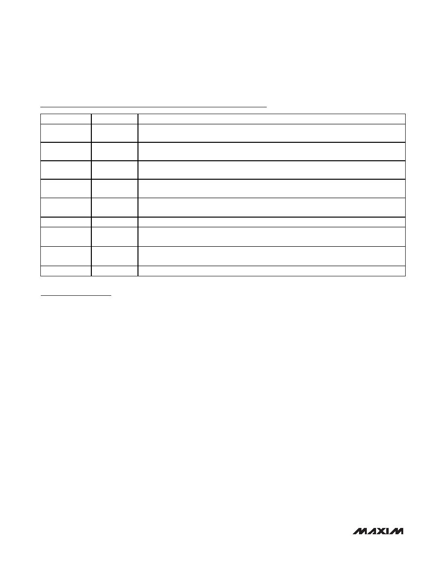
Pin Description (continued)
PIN
NAME
FUNCTION
41
D6A/B
Three-State Digital Output, Bit 6. Depending on status of A/B, output data reflects channel A
or channel B data.
42
D7A/B
Three-State Digital Output, Bit 7. Depending on status of A/B, output data reflects channel A
or channel B data.
43
D8A/B
Three-State Digital Output, Bit 8. Depending on status of A/B, output data reflects channel A
or channel B data.
44
D9A/B
Three-State Digital Output, Bit 9 (MSB). Depending on status of A/B, output data reflects
channel A or channel B data.
45
REFOUT
Internal Reference Voltage Output. May be connected to REFIN through a resistor or a
resistor-divider.
46
REFIN
Reference Input. VREFIN = 2 x (VREFP - VREFN). Bypass to GND with a > 1nF capacitor.
47
REFP
Positive Reference Input/Output. Conversion range is
± (VREFP - VREFN). Bypass to GND with
a > 0.1F capacitor.
48
REFN
Negative Reference Input/Output. Conversion range is
± (VREFP - VREFN). Bypass to GND with
a > 0.1F capacitor.
—
EP
Exposed Pad. Connect to analog ground.
相关PDF资料 |
PDF描述 |
|---|---|
| MS27497T16F99PB | CONN RCPT 23POS WALL MNT W/PINS |
| IDT723644L12PF8 | IC FIFO SYNC 2048X36 128QFP |
| V300B36M250BG3 | CONVERTER MOD DC/DC 36V 250W |
| MS27484E14B15SD | CONN PLUG 15POS STRAIGHT W/SCKT |
| MS27508E12F35SC | CONN RCPT 22POS BOX MNT W/SCKT |
相关代理商/技术参数 |
参数描述 |
|---|---|
| MAX1186ECM | 制造商:Rochester Electronics LLC 功能描述: 制造商:Maxim Integrated Products 功能描述: |
| MAX1186ECM+D | 功能描述:模数转换器 - ADC 10-Bit 2Ch 40Msps High Speed ADC RoHS:否 制造商:Texas Instruments 通道数量:2 结构:Sigma-Delta 转换速率:125 SPs to 8 KSPs 分辨率:24 bit 输入类型:Differential 信噪比:107 dB 接口类型:SPI 工作电源电压:1.7 V to 3.6 V, 2.7 V to 5.25 V 最大工作温度:+ 85 C 安装风格:SMD/SMT 封装 / 箱体:VQFN-32 |
| MAX1186ECM+TD | 功能描述:模数转换器 - ADC 10-Bit 2Ch 40Msps High Speed ADC RoHS:否 制造商:Texas Instruments 通道数量:2 结构:Sigma-Delta 转换速率:125 SPs to 8 KSPs 分辨率:24 bit 输入类型:Differential 信噪比:107 dB 接口类型:SPI 工作电源电压:1.7 V to 3.6 V, 2.7 V to 5.25 V 最大工作温度:+ 85 C 安装风格:SMD/SMT 封装 / 箱体:VQFN-32 |
| MAX1186ECM-D | 功能描述:模数转换器 - ADC RoHS:否 制造商:Texas Instruments 通道数量:2 结构:Sigma-Delta 转换速率:125 SPs to 8 KSPs 分辨率:24 bit 输入类型:Differential 信噪比:107 dB 接口类型:SPI 工作电源电压:1.7 V to 3.6 V, 2.7 V to 5.25 V 最大工作温度:+ 85 C 安装风格:SMD/SMT 封装 / 箱体:VQFN-32 |
| MAX1186ECM-TD | 功能描述:模数转换器 - ADC RoHS:否 制造商:Texas Instruments 通道数量:2 结构:Sigma-Delta 转换速率:125 SPs to 8 KSPs 分辨率:24 bit 输入类型:Differential 信噪比:107 dB 接口类型:SPI 工作电源电压:1.7 V to 3.6 V, 2.7 V to 5.25 V 最大工作温度:+ 85 C 安装风格:SMD/SMT 封装 / 箱体:VQFN-32 |
发布紧急采购,3分钟左右您将得到回复。