- 您现在的位置:买卖IC网 > PDF目录10499 > MAX1191ETI+ (Maxim Integrated Products)IC ADC 8BIT 7.5MSPS DUAL 28-TQFN PDF资料下载
参数资料
| 型号: | MAX1191ETI+ |
| 厂商: | Maxim Integrated Products |
| 文件页数: | 6/27页 |
| 文件大小: | 0K |
| 描述: | IC ADC 8BIT 7.5MSPS DUAL 28-TQFN |
| 产品培训模块: | Lead (SnPb) Finish for COTS Obsolescence Mitigation Program |
| 标准包装: | 60 |
| 位数: | 8 |
| 采样率(每秒): | 7.5M |
| 数据接口: | 并联 |
| 转换器数目: | 2 |
| 电压电源: | 单电源 |
| 工作温度: | -40°C ~ 85°C |
| 安装类型: | 表面贴装 |
| 封装/外壳: | 28-WFQFN 裸露焊盘 |
| 供应商设备封装: | 28-TQFN-EP(5x5) |
| 包装: | 管件 |
| 输入数目和类型: | 4 个单端,双极;2 个差分,双极 |
| 产品目录页面: | 1396 (CN2011-ZH PDF) |
第1页第2页第3页第4页第5页当前第6页第7页第8页第9页第10页第11页第12页第13页第14页第15页第16页第17页第18页第19页第20页第21页第22页第23页第24页第25页第26页第27页
MAX1191
Ultra-Low-Power, 7.5Msps, Dual 8-Bit ADC
14
______________________________________________________________________________________
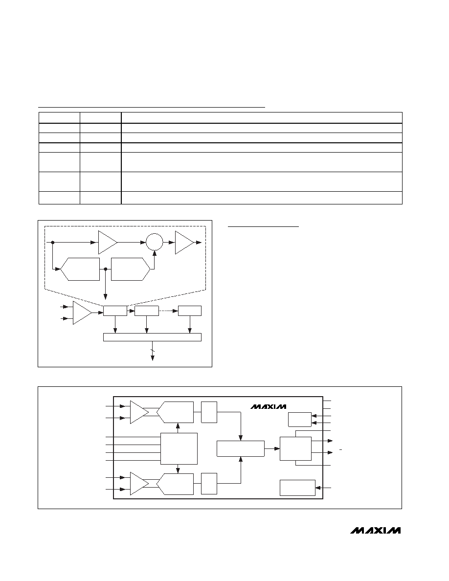
Detailed Description
The MAX1191 uses a seven-stage, fully differential,
pipelined architecture (Figure 1) that allows for high-
speed conversion while minimizing power consump-
tion. Samples taken at the inputs move progressively
through the pipeline stages every half-clock cycle.
Including the delay through the output latch, the total
clock-cycle latency is 5 clock cycles for channel A and
5.5 clock cycles for channel B.
At each stage, flash ADCs convert the held input volt-
ages into a digital code. The following digital-to-analog
converter (DAC) converts the digitized result back into
an analog voltage, which is then subtracted from the
original held input signal. The resulting error signal is
then multiplied by two, and the product is passed along
to the next pipeline stage where the process is repeated
until the signal has been processed by all stages. Digital
error correction compensates for ADC comparator off-
sets in each pipeline stage and ensures no missing
codes. Figure 2 shows the MAX1191 functional diagram.
Pin Description (continued)
PIN
NAME
FUNCTION
23
PD0
Power-Down Digital Input 0. See Table 3.
24
REFIN
Reference Input. Internally pulled up to VDD.
25
COM
Common-Mode Voltage I/O. Bypass COM to GND with a 0.33F capacitor.
26
REFN
Negative Reference I/O. Conversion range is ±(VREFP - VREFN). Bypass REFN to GND with a 0.33F
capacitor.
27
REFP
Positive Reference I/O. Conversion range is ±(VREFP - VREFN). Bypass REFP to GND with a 0.33F
capacitor.
—
EP
Exposed Paddle. Internally connected to pin 3. Externally connect EP to GND.
INA+
INA-
T/H
DIGITAL ERROR CORRECTION
D0–D7
FLASH
ADC
T/H
DAC
∑
-
+
x2
1.5 BITS
STAGE 1
STAGE 2
STAGE 7
Figure 1. Pipeline Architecture—Stage Blocks
INA+
INA-
DEC
/
T/H
INB+
INB-
DEC
/
T/H
/
REFERENCE
SYSTEM AND
BIAS
CIRCUITS
PIPELINE
ADC
A
COM
REFIN
REFN
REFP
CLK
TIMING
OVDD
OGND
MULTIPLEXER
OUTPUT
DRIVERS
POWER
CONTROL
D0–D7
/
VDD
GND
A/B
PD0
PD1
PIPELINE
ADC
B
MAX1191
Figure 2. MAX1191 Functional Diagram
相关PDF资料 |
PDF描述 |
|---|---|
| MS3102C24-12S | CONN RCPT 5POS BOX MNT W/SCKT |
| VI-BTX-MX-F4 | CONVERTER MOD DC/DC 5.2V 75W |
| MAX1063BCEG+ | IC ADC 10-BIT 250KSPS 24-QSOP |
| MS3101E18-3S | CONN RCPT 2POS FREE HNG W/SCKT |
| VI-BTX-MX-F2 | CONVERTER MOD DC/DC 5.2V 75W |
相关代理商/技术参数 |
参数描述 |
|---|---|
| MAX1191ETI+ | 功能描述:模数转换器 - ADC 8-Bit 2Ch 7.5Msps 3.6V Precision ADC RoHS:否 制造商:Texas Instruments 通道数量:2 结构:Sigma-Delta 转换速率:125 SPs to 8 KSPs 分辨率:24 bit 输入类型:Differential 信噪比:107 dB 接口类型:SPI 工作电源电压:1.7 V to 3.6 V, 2.7 V to 5.25 V 最大工作温度:+ 85 C 安装风格:SMD/SMT 封装 / 箱体:VQFN-32 |
| MAX1191ETI+T | 功能描述:模数转换器 - ADC 8-Bit 2Ch 7.5Msps 3.6V Precision ADC RoHS:否 制造商:Texas Instruments 通道数量:2 结构:Sigma-Delta 转换速率:125 SPs to 8 KSPs 分辨率:24 bit 输入类型:Differential 信噪比:107 dB 接口类型:SPI 工作电源电压:1.7 V to 3.6 V, 2.7 V to 5.25 V 最大工作温度:+ 85 C 安装风格:SMD/SMT 封装 / 箱体:VQFN-32 |
| MAX1191ETI-T | 功能描述:模数转换器 - ADC RoHS:否 制造商:Texas Instruments 通道数量:2 结构:Sigma-Delta 转换速率:125 SPs to 8 KSPs 分辨率:24 bit 输入类型:Differential 信噪比:107 dB 接口类型:SPI 工作电源电压:1.7 V to 3.6 V, 2.7 V to 5.25 V 最大工作温度:+ 85 C 安装风格:SMD/SMT 封装 / 箱体:VQFN-32 |
| MAX1192ETI | 功能描述:模数转换器 - ADC RoHS:否 制造商:Texas Instruments 通道数量:2 结构:Sigma-Delta 转换速率:125 SPs to 8 KSPs 分辨率:24 bit 输入类型:Differential 信噪比:107 dB 接口类型:SPI 工作电源电压:1.7 V to 3.6 V, 2.7 V to 5.25 V 最大工作温度:+ 85 C 安装风格:SMD/SMT 封装 / 箱体:VQFN-32 |
| MAX1192ETI+ | 功能描述:模数转换器 - ADC 8-Bit 2Ch 22Msps 3.6V Precision ADC RoHS:否 制造商:Texas Instruments 通道数量:2 结构:Sigma-Delta 转换速率:125 SPs to 8 KSPs 分辨率:24 bit 输入类型:Differential 信噪比:107 dB 接口类型:SPI 工作电源电压:1.7 V to 3.6 V, 2.7 V to 5.25 V 最大工作温度:+ 85 C 安装风格:SMD/SMT 封装 / 箱体:VQFN-32 |
发布紧急采购,3分钟左右您将得到回复。