- 您现在的位置:买卖IC网 > PDF目录2008 > MAX1191ETI+T (Maxim Integrated Products)IC ADC 8BIT 7.5MSPS DL 28-TQFN PDF资料下载
参数资料
| 型号: | MAX1191ETI+T |
| 厂商: | Maxim Integrated Products |
| 文件页数: | 9/27页 |
| 文件大小: | 0K |
| 描述: | IC ADC 8BIT 7.5MSPS DL 28-TQFN |
| 产品培训模块: | Lead (SnPb) Finish for COTS Obsolescence Mitigation Program |
| 标准包装: | 2,500 |
| 位数: | 8 |
| 采样率(每秒): | 7.5M |
| 数据接口: | 并联 |
| 转换器数目: | 2 |
| 电压电源: | 单电源 |
| 工作温度: | -40°C ~ 85°C |
| 安装类型: | 表面贴装 |
| 封装/外壳: | 28-WFQFN 裸露焊盘 |
| 供应商设备封装: | 28-TQFN-EP(5x5) |
| 包装: | 带卷 (TR) |
| 输入数目和类型: | 4 个单端,双极;2 个差分,双极 |
第1页第2页第3页第4页第5页第6页第7页第8页当前第9页第10页第11页第12页第13页第14页第15页第16页第17页第18页第19页第20页第21页第22页第23页第24页第25页第26页第27页
MAX1191
Ultra-Low-Power, 7.5Msps, Dual 8-Bit ADC
______________________________________________________________________________________
17
provide lowest possible jitter. Any significant aperture
jitter would limit the SNR performance of the on-chip
ADCs as follows:
where fIN represents the analog input frequency and
tAJ is the time of the aperture jitter.
Clock jitter is especially critical for undersampling
applications. The clock input should always be consid-
ered as an analog input and routed away from any ana-
log input or other digital signal lines. The MAX1191
clock input operates with a VDD/2 voltage threshold
and accepts a 50% ±10% duty cycle (see Typical
Operating Characteristics).
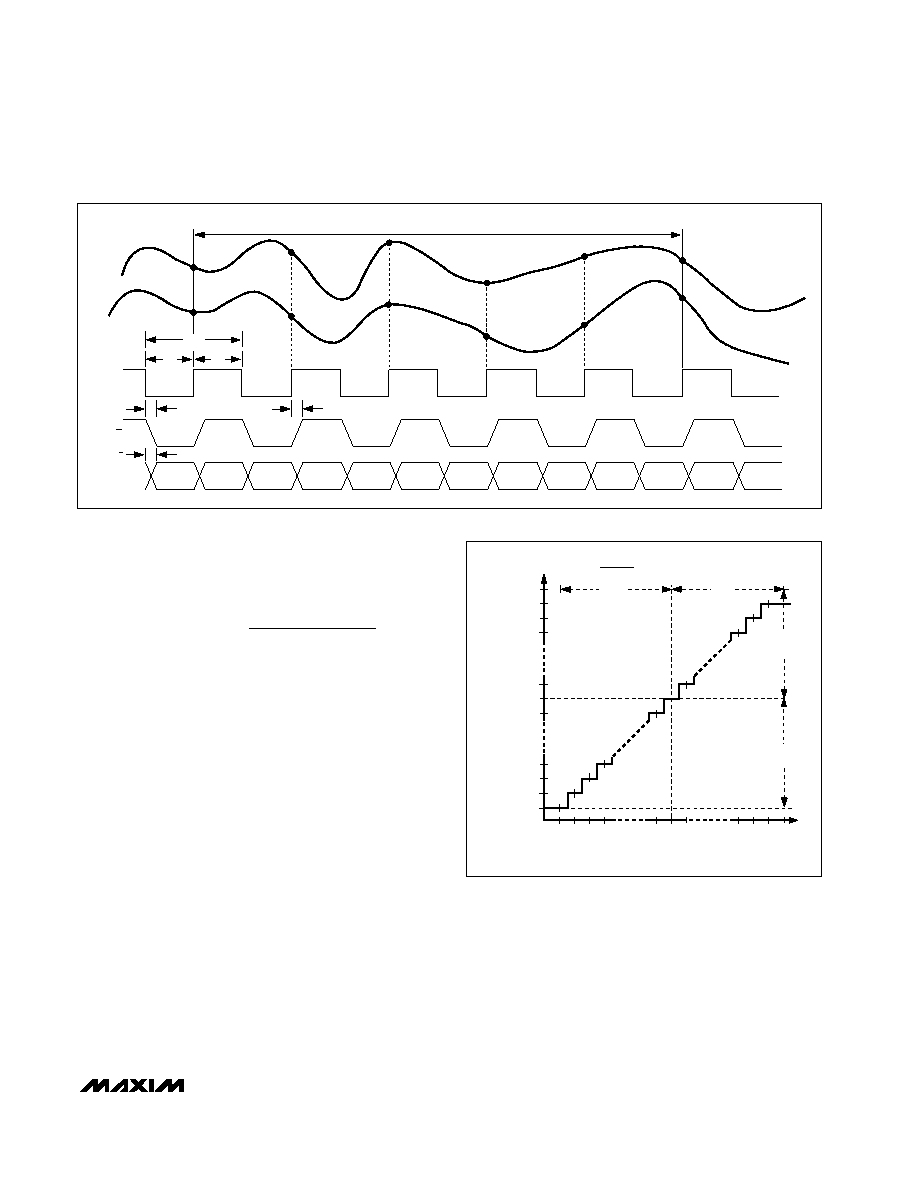
System Timing Requirements
Figure 5 shows the relationship between the clock, ana-
log inputs, A/
B indicator, and the resulting output data.
Channel A (CHA) and channel B (CHB) are simultane-
ously sampled on the rising edge of the clock signal
(CLK) and the resulting data is multiplexed at the out-
put. CHA data is updated on the rising edge and CHB
data is updated on the falling edge of the CLK. The A/
B
indicator follows CLK with a typical delay time of 6ns
and remains high when CHA data is updated and low
when CHB data is updated. Including the delay
through the output latch, the total clock-cycle latency is
5 clock cycles for CHA and 5.5 clock cycles for CHB.
Digital Output Data (D0–D7),
Channel Data Indicator (A/
B
B)
D0–D7 and A/
B are TTL/CMOS-logic compatible. The
digital output coding is offset binary (Table 2, Figure 6).
The capacitive load on the digital outputs D0–D7
should be kept as low as possible (<15pF) to avoid
large digital currents feeding back into the analog por-
tion of the MAX1191 and degrading its dynamic perfor-
mance. Buffers on the digital outputs isolate them from
SNR
ft
IN
AJ
log
=×
××
×
20
1
2
π
tDOB
tCL
tCH
tCLK
tDOA
tDA/B
5 CLOCK-CYCLE LATENCY (CHA), 5.5 CLOCK-CYCLE LATENCY (CHB)
A/B
CHB
D0–D7
D0B
CHA
D1A
CHB
D1B
CHA
D2A
CHB
D2B
CHA
D3A
CHB
D3B
CHA
D4A
CHB
D4B
CHA
D5A
CHB
D5B
CHA
D6A
CHB
D6B
CHA
CHB
CLK
Figure 5. System Timing Diagram
Figure 6. Transfer Function
INPUT VOLTAGE (LSB)
-1
-126 -125
256
2 x VREF
1LSB =
VREF = VREFP - VREFN
VREF
V
REF
V
REF
0+1
-127
+126
+128
+127
-128
+125
(COM)
OFFSET
BINAR
Y
OUTPUT
CODE
(LSB)
0000 0000
0000 0001
0000 0010
0000 0011
1111 1111
1111 1110
1111 1101
0111 1111
1000 0000
1000 0001
相关PDF资料 |
PDF描述 |
|---|---|
| MAX1192ETI+T | IC ADC 8BIT 22MSPS DL 28-TQFN |
| MAX1195ECM+TD | IC ADC 8BIT 40MSPS DL 48-TQFP |
| MAX1197ECM+TD | IC ADC 8BIT 60MSPS DL 48-TQFP |
| MAX1202AEPP+ | IC ADC 12BIT 8CH 20-DIP |
| MAX121EAP+ | IC ADC 14BIT 308KSPS 20SSOP |
相关代理商/技术参数 |
参数描述 |
|---|---|
| MAX1192ETI | 功能描述:模数转换器 - ADC RoHS:否 制造商:Texas Instruments 通道数量:2 结构:Sigma-Delta 转换速率:125 SPs to 8 KSPs 分辨率:24 bit 输入类型:Differential 信噪比:107 dB 接口类型:SPI 工作电源电压:1.7 V to 3.6 V, 2.7 V to 5.25 V 最大工作温度:+ 85 C 安装风格:SMD/SMT 封装 / 箱体:VQFN-32 |
| MAX1192ETI+ | 功能描述:模数转换器 - ADC 8-Bit 2Ch 22Msps 3.6V Precision ADC RoHS:否 制造商:Texas Instruments 通道数量:2 结构:Sigma-Delta 转换速率:125 SPs to 8 KSPs 分辨率:24 bit 输入类型:Differential 信噪比:107 dB 接口类型:SPI 工作电源电压:1.7 V to 3.6 V, 2.7 V to 5.25 V 最大工作温度:+ 85 C 安装风格:SMD/SMT 封装 / 箱体:VQFN-32 |
| MAX1192ETI+T | 功能描述:模数转换器 - ADC 8-Bit 2Ch 22Msps 3.6V Precision ADC RoHS:否 制造商:Texas Instruments 通道数量:2 结构:Sigma-Delta 转换速率:125 SPs to 8 KSPs 分辨率:24 bit 输入类型:Differential 信噪比:107 dB 接口类型:SPI 工作电源电压:1.7 V to 3.6 V, 2.7 V to 5.25 V 最大工作温度:+ 85 C 安装风格:SMD/SMT 封装 / 箱体:VQFN-32 |
| MAX1192ETI-T | 功能描述:模数转换器 - ADC RoHS:否 制造商:Texas Instruments 通道数量:2 结构:Sigma-Delta 转换速率:125 SPs to 8 KSPs 分辨率:24 bit 输入类型:Differential 信噪比:107 dB 接口类型:SPI 工作电源电压:1.7 V to 3.6 V, 2.7 V to 5.25 V 最大工作温度:+ 85 C 安装风格:SMD/SMT 封装 / 箱体:VQFN-32 |
| MAX1193ETI | 功能描述:模数转换器 - ADC RoHS:否 制造商:Texas Instruments 通道数量:2 结构:Sigma-Delta 转换速率:125 SPs to 8 KSPs 分辨率:24 bit 输入类型:Differential 信噪比:107 dB 接口类型:SPI 工作电源电压:1.7 V to 3.6 V, 2.7 V to 5.25 V 最大工作温度:+ 85 C 安装风格:SMD/SMT 封装 / 箱体:VQFN-32 |
发布紧急采购,3分钟左右您将得到回复。