- 您现在的位置:买卖IC网 > PDF目录10563 > MAX1195ECM+D (Maxim Integrated Products)IC ADC 8BIT 40MSPS DL 48-TQFP PDF资料下载
参数资料
| 型号: | MAX1195ECM+D |
| 厂商: | Maxim Integrated Products |
| 文件页数: | 6/22页 |
| 文件大小: | 0K |
| 描述: | IC ADC 8BIT 40MSPS DL 48-TQFP |
| 产品培训模块: | Lead (SnPb) Finish for COTS Obsolescence Mitigation Program |
| 标准包装: | 250 |
| 位数: | 8 |
| 采样率(每秒): | 40M |
| 数据接口: | 并联 |
| 转换器数目: | 2 |
| 功率耗散(最大): | 108mW |
| 电压电源: | 单电源 |
| 工作温度: | -40°C ~ 85°C |
| 安装类型: | 表面贴装 |
| 封装/外壳: | 48-TQFP 裸露焊盘 |
| 供应商设备封装: | 48-TQFP 裸露焊盘(7x7) |
| 包装: | 托盘 |
| 输入数目和类型: | 4 个单端,双极;2 个差分,双极 |
MAX1195
where fIN represents the analog input frequency and
tAJ is the time of the aperture jitter.
Clock jitter is especially critical for undersampling
applications. The clock input should always be consid-
ered as an analog input and routed away from any ana-
log input or other digital signal lines.
The MAX1195 clock input operates with a voltage thresh-
old set to VDD/2. Clock inputs with a duty cycle other
than 50% must meet the specifications for high and low
periods as stated in the Electrical Characteristics table.
System Timing Requirements
Figure 3 depicts the relationship between the clock
input, analog input, and data output. The MAX1195
samples at the rising edge of the input clock. Output
data for channels A and B is valid on the next rising
edge of the input clock. The output data has an internal
latency of five clock cycles. Figure 3 also determines
the relationship between the input clock parameters
and the valid output data on channels A and B.
Digital Output Data (D0A/B–D7A/B), Output
Data Format Selection (T/B), Output
Enable (OE)
All digital outputs, D0A–D7A (channel A) and D0B–D7B
(channel B), are TTL/CMOS-logic compatible. There is
a five-clock-cycle latency between any particular sam-
ple and its corresponding output data. The output coding
can either be straight offset binary or two’s complement
(Table 1) controlled by a single pin (T/B). Pull T/B low to
select offset binary and high to activate two’s comple-
ment output coding. The capacitive load on the digital
outputs D0A–D7A and D0B–D7B should be kept as low
as possible (<15pF), to avoid large digital currents that
could feed back into the analog portion of the
MAX1195, thereby degrading its dynamic performance.
Using buffers on the digital outputs of the ADCs can
further isolate the digital outputs from heavy capacitive
loads. To further improve the dynamic performance of
the MAX1195, small series resistors (e.g., 100
) can
be added to the digital output paths close to the
MAX1195.
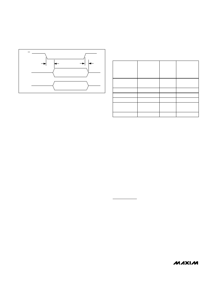
Figure 4 displays the timing relationship between out-
put enable and data output valid, as well as power-
down/wake-up and data output valid.
Power-Down and Sleep Modes
The MAX1195 offers two power-save modes—sleep
mode (SLEEP) and full power-down (PD) mode. In
sleep mode (SLEEP = 1), only the reference bias circuit
is active (both ADCs are disabled), and current con-
sumption is reduced to 3mA.
To enter full power-down mode, pull PD high. With OE
simultaneously low, all outputs are latched at the last
value prior to the power down. Pulling OE high forces
the digital outputs into a high-impedance state.
Applications Information
Figure 5 depicts a typical application circuit containing
two single-ended-to-differential converters. The internal
reference provides a VDD/2 output voltage for level-
shifting purposes. The input is buffered and then split
to a voltage follower and inverter. One lowpass filter per
amplifier suppresses some of the wideband noise
associated with high-speed operational amplifiers. The
user can select the RISO and CIN values to optimize the
filter performance, to suit a particular application. For
the application in Figure 5, a RISO of 50
is placed
before the capacitive load to prevent ringing and oscil-
lation. The 22pF CIN capacitor acts as a small filter
capacitor.
Dual, 8-Bit, 40Msps, 3V, Low-Power ADC with
Internal Reference and Parallel Outputs
14
______________________________________________________________________________________
OUTPUT
D7A–D0A
OE
tDISABLE
tENABLE
HIGH-Z
VALID DATA
OUTPUT
D7B–D0B
HIGH-Z
VALID DATA
Figure 4. Output Timing Diagram
STRAIGHT
OFFSET
BINARY
TWO’S
COMPLEMENT
DIFFERENTIAL
INPUT
VOLTAGE*
DIFFERENTIAL
INPUT
T/B = 0
T/B = 1
VREF x 255/256
+Full Scale
-1LSB
1111 1111
0111 1111
VREF x 1/256
+1LSB
1000 0001
0000 0001
0
Bipolar zero
1000 0000
0000 0000
-VREF x 1/256
-1LSB
0111 1111
1111 1111
-VREF x 255/256
-Full Scale
+1LSB
0000 0001
1000 0001
-VREF x 256/256
-Full Scale
0000 0000
1000 0000
Table 1. MAX1195 Output Codes For
Differential Inputs
*VREF = VREFP – VREFN
相关PDF资料 |
PDF描述 |
|---|---|
| LT1133ACSW#PBF | IC 3DRV/5RCV RS232 5V 24-SOIC |
| MAX1030BEEG+ | IC ADC 10BIT 300KSPS 24-QSOP |
| 206151-3 | CONN RECEPT CPC 37POS STD SER 1 |
| VE-2T4-IW-F2 | CONVERTER MOD DC/DC 48V 100W |
| VI-J1Y-MY-F4 | CONVERTER MOD DC/DC 3.3V 33W |
相关代理商/技术参数 |
参数描述 |
|---|---|
| MAX1195ECM-TD | 功能描述:模数转换器 - ADC RoHS:否 制造商:Texas Instruments 通道数量:2 结构:Sigma-Delta 转换速率:125 SPs to 8 KSPs 分辨率:24 bit 输入类型:Differential 信噪比:107 dB 接口类型:SPI 工作电源电压:1.7 V to 3.6 V, 2.7 V to 5.25 V 最大工作温度:+ 85 C 安装风格:SMD/SMT 封装 / 箱体:VQFN-32 |
| MAX1196ECM | 制造商:Rochester Electronics LLC 功能描述: 制造商:Maxim Integrated Products 功能描述: |
| MAX1196ECM+D | 功能描述:模数转换器 - ADC 8-Bit 2Ch 40Msps 3V High Speed ADC RoHS:否 制造商:Texas Instruments 通道数量:2 结构:Sigma-Delta 转换速率:125 SPs to 8 KSPs 分辨率:24 bit 输入类型:Differential 信噪比:107 dB 接口类型:SPI 工作电源电压:1.7 V to 3.6 V, 2.7 V to 5.25 V 最大工作温度:+ 85 C 安装风格:SMD/SMT 封装 / 箱体:VQFN-32 |
| MAX1196ECM+TD | 功能描述:模数转换器 - ADC 8-Bit 2Ch 40Msps 3V High Speed ADC RoHS:否 制造商:Texas Instruments 通道数量:2 结构:Sigma-Delta 转换速率:125 SPs to 8 KSPs 分辨率:24 bit 输入类型:Differential 信噪比:107 dB 接口类型:SPI 工作电源电压:1.7 V to 3.6 V, 2.7 V to 5.25 V 最大工作温度:+ 85 C 安装风格:SMD/SMT 封装 / 箱体:VQFN-32 |
| MAX1196ECM-D | 功能描述:模数转换器 - ADC RoHS:否 制造商:Texas Instruments 通道数量:2 结构:Sigma-Delta 转换速率:125 SPs to 8 KSPs 分辨率:24 bit 输入类型:Differential 信噪比:107 dB 接口类型:SPI 工作电源电压:1.7 V to 3.6 V, 2.7 V to 5.25 V 最大工作温度:+ 85 C 安装风格:SMD/SMT 封装 / 箱体:VQFN-32 |
发布紧急采购,3分钟左右您将得到回复。