- 您现在的位置:买卖IC网 > PDF目录10558 > MAX1197ECM+D (Maxim Integrated Products)IC ADC 8BIT 60MSPS DUAL 48-TQFP PDF资料下载
参数资料
| 型号: | MAX1197ECM+D |
| 厂商: | Maxim Integrated Products |
| 文件页数: | 3/22页 |
| 文件大小: | 0K |
| 描述: | IC ADC 8BIT 60MSPS DUAL 48-TQFP |
| 产品培训模块: | Lead (SnPb) Finish for COTS Obsolescence Mitigation Program |
| 标准包装: | 250 |
| 位数: | 8 |
| 采样率(每秒): | 60M |
| 数据接口: | 并联 |
| 转换器数目: | 2 |
| 功率耗散(最大): | 150mW |
| 电压电源: | 单电源 |
| 工作温度: | -40°C ~ 85°C |
| 安装类型: | 表面贴装 |
| 封装/外壳: | 48-TQFP 裸露焊盘 |
| 供应商设备封装: | 48-TQFP 裸露焊盘(7x7) |
| 包装: | 托盘 |
| 输入数目和类型: | 4 个单端,双极;2 个差分,双极 |
| 产品目录页面: | 1396 (CN2011-ZH PDF) |
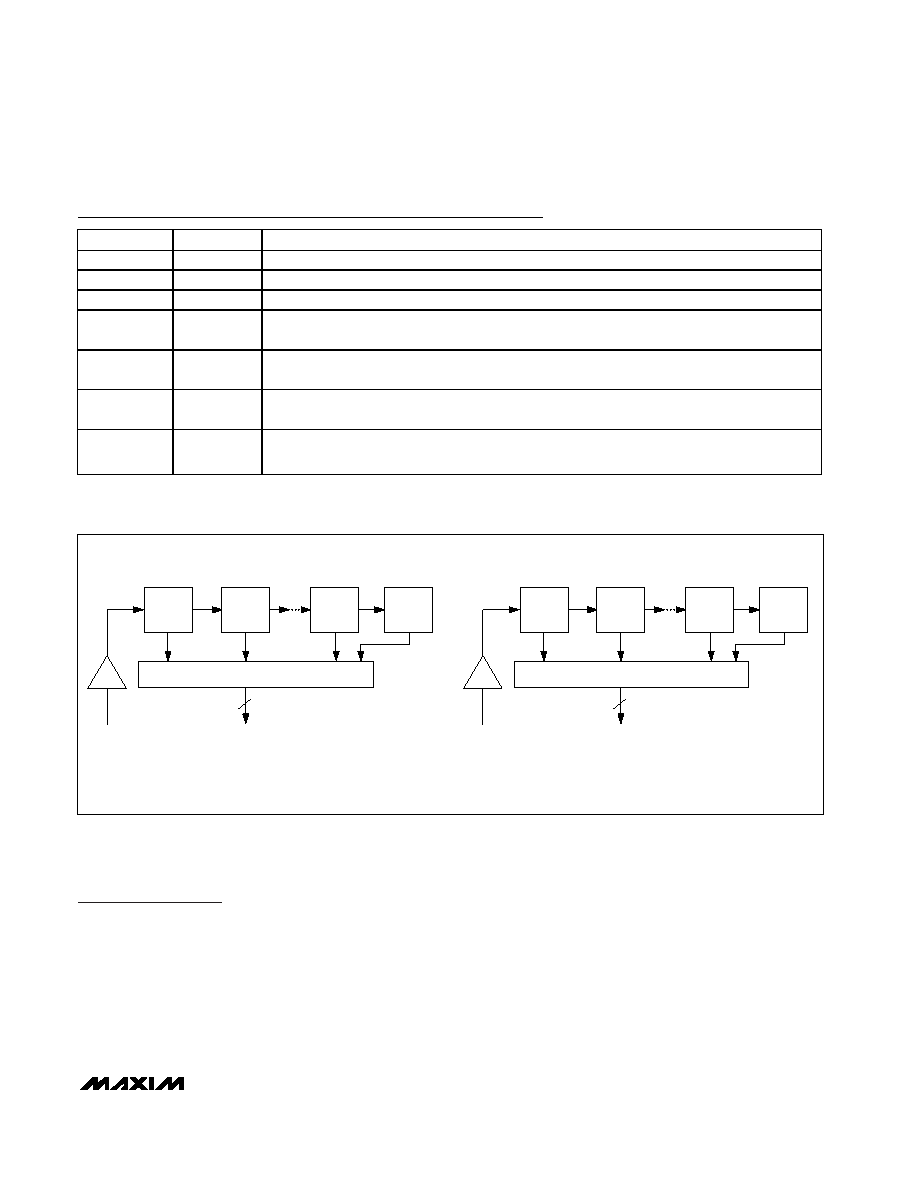
Detailed Description
The MAX1197 uses a seven-stage, fully differential,
pipelined architecture (Figure 1) that allows for high-
speed conversion while minimizing power consump-
tion. Samples taken at the inputs move progressively
through the pipeline stages every half-clock cycle.
Including the delay through the output latch, the total
clock-cycle latency is five clock cycles.
Flash ADCs convert the held input voltages into a digi-
tal code. Internal MDACs convert the digitized results
back into analog voltages, which are then subtracted
from the original held input signals. The resulting error
signals are then multiplied by two, and the residues are
passed along to the next pipeline stages where the
process is repeated until the signals have been
processed by all seven stages.
Input Track-and-Hold Circuits
Figure 2 displays a simplified functional diagram of the
input T/H circuits in both track and hold mode. In track
mode, switches S1, S2a, S2b, S4a, S4b, S5a, and S5b
MAX1197
Dual, 8-Bit, 60Msps, 3V, Low-Power ADC with
Internal Reference and Parallel Outputs
______________________________________________________________________________________
11
Pin Description (continued)
PIN
NAME
FUNCTION
42
D5A
Three-State Digital Output, Bit 5, Channel A
43
D6A
Three-State Digital Output, Bit 6, Channel A
44
D7A
Three-State Digital Output, Bit 7 (MSB), Channel A
45
REFOUT
Internal Reference Voltage Output. May be connected to REFIN through a resistor or a resistor
divider.
46
REFIN
Reference Input. VREFIN = 2 x (VREFP – VREFN).
Bypass to GND with a > 0.1F capacitor.
47
REFP
Positive Reference I/O. Conversion range is
±(VREFP – VREFN).
Bypass to GND with a > 0.1F capacitor.
48
REFN
Negative Reference I/O. Conversion range is
±(VREFP – VREFN).
Bypass to GND with a > 0.1F capacitor.
8
VINA
STAGE 1
STAGE 2
D7A–D0A
VINA = INPUT VOLTAGE BETWEEN INA+ AND INA- (DIFFERENTIAL OR SINGLE ENDED)
VINB = INPUT VOLTAGE BETWEEN INB+ AND INB- (DIFFERENTIAL OR SINGLE ENDED)
DIGITAL ALIGNMENT LOGIC
STAGE 6
STAGE 7
2-BIT FLASH
ADC
T/H
8
VINB
STAGE 1
STAGE 2
D7B–D0B
DIGITAL ALIGNMENT LOGIC
STAGE 6
STAGE 7
2-BIT FLASH
ADC
T/H
Figure 1. Pipelined Architecture—Stage Blocks
相关PDF资料 |
PDF描述 |
|---|---|
| VI-BTJ-MX-F3 | CONVERTER MOD DC/DC 36V 75W |
| VI-BTJ-MX-F2 | CONVERTER MOD DC/DC 36V 75W |
| MAX132CWG+ | IC ADC 18BIT W/SRL INTRFC 24SOIC |
| VI-BTJ-MW | CONVERTER MOD DC/DC 36V 100W |
| VI-BTH-MX-F4 | CONVERTER MOD DC/DC 52V 75W |
相关代理商/技术参数 |
参数描述 |
|---|---|
| MAX1197ECM-TD | 功能描述:模数转换器 - ADC RoHS:否 制造商:Texas Instruments 通道数量:2 结构:Sigma-Delta 转换速率:125 SPs to 8 KSPs 分辨率:24 bit 输入类型:Differential 信噪比:107 dB 接口类型:SPI 工作电源电压:1.7 V to 3.6 V, 2.7 V to 5.25 V 最大工作温度:+ 85 C 安装风格:SMD/SMT 封装 / 箱体:VQFN-32 |
| MAX1198E/D | 功能描述:模数转换器 - ADC DICE SALES DICE RoHS:否 制造商:Texas Instruments 通道数量:2 结构:Sigma-Delta 转换速率:125 SPs to 8 KSPs 分辨率:24 bit 输入类型:Differential 信噪比:107 dB 接口类型:SPI 工作电源电压:1.7 V to 3.6 V, 2.7 V to 5.25 V 最大工作温度:+ 85 C 安装风格:SMD/SMT 封装 / 箱体:VQFN-32 |
| MAX1198ECM+D | 功能描述:模数转换器 - ADC 8-Bit 2Ch 100Msps 3.3V High Speed ADC RoHS:否 制造商:Texas Instruments 通道数量:2 结构:Sigma-Delta 转换速率:125 SPs to 8 KSPs 分辨率:24 bit 输入类型:Differential 信噪比:107 dB 接口类型:SPI 工作电源电压:1.7 V to 3.6 V, 2.7 V to 5.25 V 最大工作温度:+ 85 C 安装风格:SMD/SMT 封装 / 箱体:VQFN-32 |
| MAX1198ECM+TD | 功能描述:模数转换器 - ADC 8-Bit 2Ch 100Msps 3.3V High Speed ADC RoHS:否 制造商:Texas Instruments 通道数量:2 结构:Sigma-Delta 转换速率:125 SPs to 8 KSPs 分辨率:24 bit 输入类型:Differential 信噪比:107 dB 接口类型:SPI 工作电源电压:1.7 V to 3.6 V, 2.7 V to 5.25 V 最大工作温度:+ 85 C 安装风格:SMD/SMT 封装 / 箱体:VQFN-32 |
| MAX1198ECM-D | 功能描述:模数转换器 - ADC RoHS:否 制造商:Texas Instruments 通道数量:2 结构:Sigma-Delta 转换速率:125 SPs to 8 KSPs 分辨率:24 bit 输入类型:Differential 信噪比:107 dB 接口类型:SPI 工作电源电压:1.7 V to 3.6 V, 2.7 V to 5.25 V 最大工作温度:+ 85 C 安装风格:SMD/SMT 封装 / 箱体:VQFN-32 |
发布紧急采购,3分钟左右您将得到回复。