- 您现在的位置:买卖IC网 > PDF目录9909 > MAX1230BETI+T (Maxim Integrated Products)IC ADC 12BIT 300KSPS 28-TQFN PDF资料下载
参数资料
| 型号: | MAX1230BETI+T |
| 厂商: | Maxim Integrated Products |
| 文件页数: | 3/23页 |
| 文件大小: | 0K |
| 描述: | IC ADC 12BIT 300KSPS 28-TQFN |
| 产品培训模块: | Lead (SnPb) Finish for COTS Obsolescence Mitigation Program |
| 标准包装: | 2,500 |
| 位数: | 12 |
| 采样率(每秒): | 300k |
| 数据接口: | MICROWIRE?,QSPI?,串行,SPI? |
| 转换器数目: | 1 |
| 功率耗散(最大): | 1.67W |
| 电压电源: | 单电源 |
| 工作温度: | -40°C ~ 85°C |
| 安装类型: | 表面贴装 |
| 封装/外壳: | 28-WFQFN 裸露焊盘 |
| 供应商设备封装: | 28-TQFN-EP(5x5) |
| 包装: | 带卷 (TR) |
| 输入数目和类型: | 16 个单端,单极;16 个单端,双极;8 个差分,单极;8 个差分,双极 |
MAX1226/MAX1228/MAX1230
12-Bit 300ksps ADCs with FIFO,
Temp Sensor, Internal Reference
______________________________________________________________________________________
11
appropriate bit of the bipolar or unipolar register.
Unipolar mode sets the differential input range from 0 to
VREF. A negative differential analog input in unipolar
mode causes the digital output code to be zero.
Selecting bipolar mode sets the differential input range
to ±VREF / 2. The digital output code is binary in unipo-
lar mode and two’s complement in bipolar mode. (See
the transfer function graphs, Figures 8 and 9.)
In single-ended mode, the MAX1226/MAX1228/
MAX1230 always operate in unipolar mode. The analog
inputs are internally referenced to GND with a full-scale
input range from 0 to VREF.
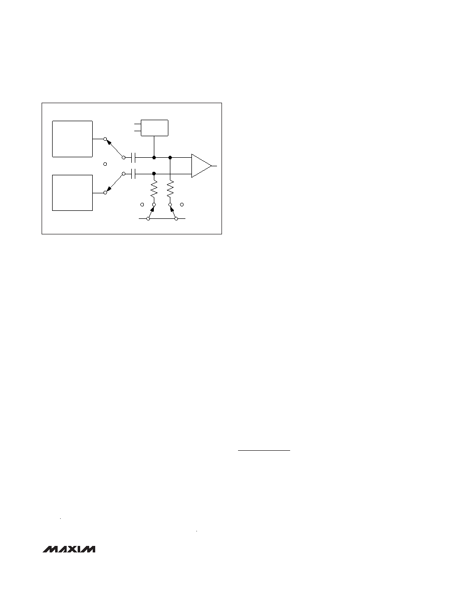
True Differential Analog Input T/H
The equivalent circuit of Figure 3 shows the
MAX1226/MAX1228/MAX1230s’ input architecture. In
track mode, a positive input capacitor is connected to
AIN0–AIN15 in single-ended mode (and AIN0, AIN2,
AIN4…AIN14 in differential mode). A negative input
capacitor is connected to GND in single-ended mode
(or AIN1, AIN3, AIN5…AIN15 in differential mode). For
external track-and-hold timing, use clock mode 01.
After the T/H enters hold mode, the difference between
the sampled positive and negative input voltages is
converted. The time required for the T/H to acquire an
input signal is determined by how quickly its input
capacitance is charged. If the input signal’s source
impedance is high, the required acquisition time length-
ens. The acquisition time, tACQ, is the maximum time
needed for a signal to be acquired, plus the power-up
time. It is calculated by the following equation:
where RIN = 1.5k, RS is the source impedance of the
input signal, and tPWR = 1s, the power-up time of the
device. The varying power-up times are detailed in the
explanation of the clock mode conversions.
tACQ is never less than 1.4s, and any source imped-
ance below 300 does not significantly affect the
ADC’s AC performance. A high-impedance source can
be accommodated either by lengthening tACQ or by
placing a 1F capacitor between the positive and neg-
ative analog inputs.
Internal FIFO
The MAX1226/MAX1228/MAX1230 contain a FIFO
buffer that can hold up to 16 ADC results plus one tem-
perature result. This allows the ADC to handle multiple
internally clocked conversions and a temperature mea-
surement, without tying up the serial bus.
If the FIFO is filled and further conversions are request-
ed without reading from the FIFO, the oldest ADC
results are overwritten by the new ADC results. Each
result contains 2 bytes, with the MSB preceded by 4
leading zeros. After each falling edge of CS, the oldest
available byte of data is available at DOUT, MSB first.
When the FIFO is empty, DOUT is zero.
The first 2 bytes of data read out after a temperature mea-
surement always contain the temperature result preceded
by 4 leading zeros, MSB first. If another temperature mea-
surement is performed before the first temperature result
is read out, the old measurement is overwritten by the
new result. Temperature results are in degrees Celsius
(two’s complement) at a resolution of 1/8 of degree. See
the
Temperature Measurements section for details on
converting the digital code to a temperature.
Internal Clock
The MAX1226/MAX1228/MAX1230 operate from an inter-
nal oscillator, which is accurate within 10% of the 4.4MHz
nominal clock rate. The internal oscillator is active in clock
modes 00, 01, and 10. Read out the data at clock speeds
up to 10MHz. See Figures 4–7 for details on timing speci-
fications and starting a conversion.
Applications Information
Register Descriptions
The MAX1226/MAX1228/MAX1230 communicate
between the internal registers and the external circuitry
through the SPI-/QSPI-compatible serial interface.
Table 1 details the registers and the bit names. Tables
2–7 show the various functions within the conversion
register, setup register, averaging register, reset regis-
ter, unipolar register, and bipolar register.
tx R
R
x
pF
t
AQC
S
IN
PWR
=+
()
+
924
+
-
HOLD
CIN+
REF
GND
DAC
CIN-
VDD/2
COMPARATOR
AIN0-AIN15
(SINGLE ENDED);
AIN0, AIN2,
AIN4…AIN14
(DIFFERENTIAL)
GND
(SINGLE ENDED);
AIN1, AIN3,
AIN5…AIN15
(DIFFERENTIAL)
HOLD
Figure 3. Equivalent Input Circuit
相关PDF资料 |
PDF描述 |
|---|---|
| MS27484T18A11SB | CONN PLUG 11POS STRAIGHT W/SCKT |
| MAX1231BETI+T | IC ADC 12BIT 300KSPS 28-TQFN |
| MS27468T21F39S | CONN RCPT 39POS JAM NUT W/SCKT |
| MAX152CPP+ | IC ADC 8BIT 1UA PWR-DWN 20-DIP |
| VE-2NV-CU-B1 | CONVERTER MOD DC/DC 5.8V 200W |
相关代理商/技术参数 |
参数描述 |
|---|---|
| MAX1231ACEG | 功能描述:模数转换器 - ADC RoHS:否 制造商:Texas Instruments 通道数量:2 结构:Sigma-Delta 转换速率:125 SPs to 8 KSPs 分辨率:24 bit 输入类型:Differential 信噪比:107 dB 接口类型:SPI 工作电源电压:1.7 V to 3.6 V, 2.7 V to 5.25 V 最大工作温度:+ 85 C 安装风格:SMD/SMT 封装 / 箱体:VQFN-32 |
| MAX1231ACEG+ | 功能描述:模数转换器 - ADC 12-Bit 16Ch 300ksps 3.6V Precision ADC RoHS:否 制造商:Texas Instruments 通道数量:2 结构:Sigma-Delta 转换速率:125 SPs to 8 KSPs 分辨率:24 bit 输入类型:Differential 信噪比:107 dB 接口类型:SPI 工作电源电压:1.7 V to 3.6 V, 2.7 V to 5.25 V 最大工作温度:+ 85 C 安装风格:SMD/SMT 封装 / 箱体:VQFN-32 |
| MAX1231ACEG+T | 功能描述:模数转换器 - ADC RoHS:否 制造商:Texas Instruments 通道数量:2 结构:Sigma-Delta 转换速率:125 SPs to 8 KSPs 分辨率:24 bit 输入类型:Differential 信噪比:107 dB 接口类型:SPI 工作电源电压:1.7 V to 3.6 V, 2.7 V to 5.25 V 最大工作温度:+ 85 C 安装风格:SMD/SMT 封装 / 箱体:VQFN-32 |
| MAX1231ACEG-T | 功能描述:模数转换器 - ADC RoHS:否 制造商:Texas Instruments 通道数量:2 结构:Sigma-Delta 转换速率:125 SPs to 8 KSPs 分辨率:24 bit 输入类型:Differential 信噪比:107 dB 接口类型:SPI 工作电源电压:1.7 V to 3.6 V, 2.7 V to 5.25 V 最大工作温度:+ 85 C 安装风格:SMD/SMT 封装 / 箱体:VQFN-32 |
| MAX1231AEEG | 功能描述:模数转换器 - ADC RoHS:否 制造商:Texas Instruments 通道数量:2 结构:Sigma-Delta 转换速率:125 SPs to 8 KSPs 分辨率:24 bit 输入类型:Differential 信噪比:107 dB 接口类型:SPI 工作电源电压:1.7 V to 3.6 V, 2.7 V to 5.25 V 最大工作温度:+ 85 C 安装风格:SMD/SMT 封装 / 箱体:VQFN-32 |
发布紧急采购,3分钟左右您将得到回复。