- 您现在的位置:买卖IC网 > PDF目录17007 > MAX1231BEVKIT# (Maxim Integrated Products)KIT EVALUATION FOR 12BIT ADCS PDF资料下载
参数资料
| 型号: | MAX1231BEVKIT# |
| 厂商: | Maxim Integrated Products |
| 文件页数: | 3/22页 |
| 文件大小: | 0K |
| 描述: | KIT EVALUATION FOR 12BIT ADCS |
| 产品培训模块: | Lead (SnPb) Finish for COTS Obsolescence Mitigation Program |
| 标准包装: | 1 |
| ADC 的数量: | 1 |
| 位数: | 12 |
| 采样率(每秒): | 300k |
| 数据接口: | SPI? |
| 输入范围: | ±VREF/2 |
| 工作温度: | 0°C ~ 70°C |
| 已用 IC / 零件: | MAX1231 |
| 已供物品: | 板 |
MAX1227/MAX1229/MAX1231
12-Bit 300ksps ADCs with FIFO,
Temp Sensor, Internal Reference
______________________________________________________________________________________
11
Unipolar/Bipolar
Address the unipolar and bipolar registers through the
setup register (bits 1 and 0). Program a pair of analog
channels for differential operation by writing a 1 to the
appropriate bit of the bipolar or unipolar register.
Unipolar mode sets the differential input range from 0
to VREF. A negative differential analog input in unipolar
mode causes the digital output code to be zero.
Selecting bipolar mode sets the differential input range
to ±VREF/2. The digital output code is binary in unipolar
mode and two’s complement in bipolar mode (Figures
8 and 9).
In single-ended mode, the MAX1227/MAX1229/
MAX1231 always operate in unipolar mode. The analog
inputs are internally referenced to GND with a full-scale
input range from 0 to VREF.
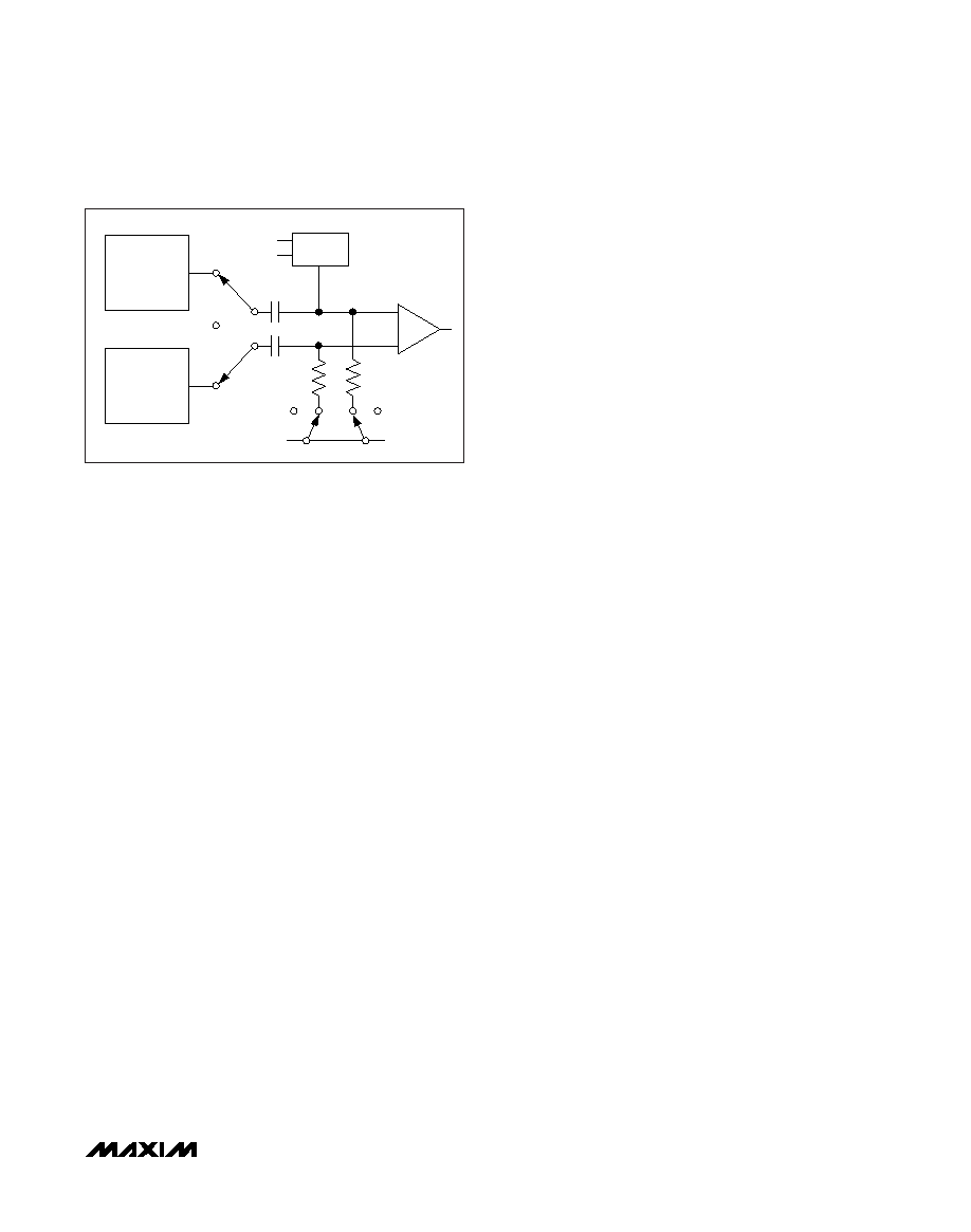
True Differential Analog Input T/H
The equivalent circuit of Figure 3 shows the MAX1227/
MAX1229/MAX1231s’ input architecture. In track mode,
a positive input capacitor is connected to AIN0–AIN15
in single-ended mode (and AIN0, AIN2, AIN4…AIN14
in differential mode). A negative input capacitor is con-
nected to GND in single-ended mode (or AIN1, AIN3,
AIN5…AIN15 in differential mode). For external T/H
timing, use clock mode 01. After the T/H enters hold
mode, the difference between the sampled positive
and negative input voltages is converted. The time
required for the T/H to acquire an input signal is deter-
mined by how quickly its input capacitance is charged.
If the input signal’s source impedance is high, the
required acquisition time lengthens. The acquisition
time, tACQ, is the maximum time needed for a signal to
be acquired, plus the power-up time. It is calculated by
the following equation:
where RIN = 1.5k
, RS is the source impedance of the
input signal, and tPWR = 1s, the power-up time of the
device. The varying power-up times are detailed in the
explanation of the clock mode conversions.
tACQ is never less than 1.4s, and any source imped-
ance below 300
does not significantly affect the
ADC’s AC performance. A high-impedance source can
be accommodated either by lengthening tACQ or by
placing a 1F capacitor between the positive and neg-
ative analog inputs.
Internal FIFO
The MAX1227/MAX1229/MAX1231 contain a FIFO
buffer that can hold up to 16 ADC results plus one tem-
perature result. This allows the ADC to handle multiple
internally clocked conversions and a temperature mea-
surement, without tying up the serial bus.
If the FIFO is filled and further conversions are request-
ed without reading from the FIFO, the oldest ADC
results are overwritten by the new ADC results. Each
result contains 2 bytes, with the MSB preceded by four
leading zeros. After each falling edge of CS, the oldest
available byte of data is available at DOUT, MSB first.
When the FIFO is empty, DOUT is zero.
The first 2 bytes of data read out after a temperature
measurement always contain the temperature result
preceded by four leading zeros, MSB first. If another
temperature measurement is performed before the first
temperature result is read out, the old measurement is
overwritten by the new result. Temperature results are
in degrees Celsius (two’s complement) at a resolution
of 1/8 of a degree. See the
Temperature Measurements
section for details on converting the digital code to a
temperature.
Internal Clock
The MAX1227/MAX1229/MAX1231 operate from an
internal oscillator, which is accurate within 10% of the
4.4MHz nominal clock rate. The internal oscillator is
active in clock modes 00, 01, and 10. Read out the
data at clock speeds up to 10MHz. See Figures
4–7 for details on timing specifications and starting a
conversion.
tx R
R
x
pF
t
ACQ
S
IN
PWR
=+
+
()
924
+
-
HOLD
CIN+
REF
GND
DAC
CIN-
VDD/2
COMPARATOR
AIN0-AIN15
(SINGLE ENDED);
AIN0, AIN2,
AIN4…AIN14
(DIFFERENTIAL)
GND
(SINGLE ENDED);
AIN1, AIN3,
AIN5…AIN15
(DIFFERENTIAL)
HOLD
Figure 3. Equivalent Input Circuit
相关PDF资料 |
PDF描述 |
|---|---|
| SDR1105-470KL | INDUCTOR POWER 47UH 10% SMD |
| GSM11DSEH-S13 | CONN EDGECARD 22POS .156 EXTEND |
| 101-0437 | CARD DGTL IO 16/8 SOURCNG SR9205 |
| 0210490250 | CABLE JUMPER 1.25MM .229M 18POS |
| 0210490249 | CABLE JUMPER 1.25MM .229M 18POS |
相关代理商/技术参数 |
参数描述 |
|---|---|
| MAX1231BEVKIT# | 功能描述:数据转换 IC 开发工具 MAX1231 Eval Kit RoHS:否 制造商:Texas Instruments 产品:Demonstration Kits 类型:ADC 工具用于评估:ADS130E08 接口类型:SPI 工作电源电压:- 6 V to + 6 V |
| MAX1231BEVSYS# | 功能描述:数据转换 IC 开发工具 MAX1231 Eval Kit RoHS:否 制造商:Texas Instruments 产品:Demonstration Kits 类型:ADC 工具用于评估:ADS130E08 接口类型:SPI 工作电源电压:- 6 V to + 6 V |
| MAX1231EVC16 | 功能描述:数据转换 IC 开发工具 MAX1231 Eval Kit RoHS:否 制造商:Texas Instruments 产品:Demonstration Kits 类型:ADC 工具用于评估:ADS130E08 接口类型:SPI 工作电源电压:- 6 V to + 6 V |
| MAX1231EVKIT | 功能描述:数据转换 IC 开发工具 MAX1231 Eval Kit RoHS:否 制造商:Texas Instruments 产品:Demonstration Kits 类型:ADC 工具用于评估:ADS130E08 接口类型:SPI 工作电源电压:- 6 V to + 6 V |
| MAX1232C/D | 功能描述:监控电路 RoHS:否 制造商:STMicroelectronics 监测电压数: 监测电压: 欠电压阈值: 过电压阈值: 输出类型:Active Low, Open Drain 人工复位:Resettable 监视器:No Watchdog 电池备用开关:No Backup 上电复位延迟(典型值):10 s 电源电压-最大:5.5 V 最大工作温度:+ 85 C 安装风格:SMD/SMT 封装 / 箱体:UDFN-6 封装:Reel |
发布紧急采购,3分钟左右您将得到回复。