- 您现在的位置:买卖IC网 > PDF目录383314 > MAX1240BCPA (MAXIM INTEGRATED PRODUCTS INC) +2.7V, Low-Power, 12-Bit Serial ADCs in 8-Pin SO PDF资料下载
参数资料
| 型号: | MAX1240BCPA |
| 厂商: | MAXIM INTEGRATED PRODUCTS INC |
| 元件分类: | ADC |
| 英文描述: | +2.7V, Low-Power, 12-Bit Serial ADCs in 8-Pin SO |
| 中文描述: | 1-CH 12-BIT SUCCESSIVE APPROXIMATION ADC, SERIAL ACCESS, PDIP8 |
| 封装: | ROHS COMPLIANT, PLASTIC, DIP-8 |
| 文件页数: | 8/16页 |
| 文件大小: | 280K |
| 代理商: | MAX1240BCPA |
M
+2.7V, Low-Power,
12-Bit S erial ADCs in 8-Pin S O
8
_______________________________________________________________________________________
_______________Detailed Description
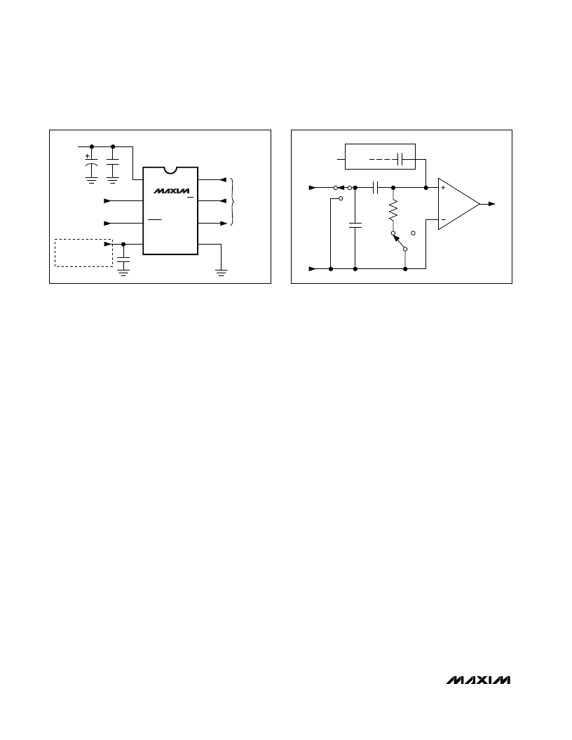
Converter Operation
The MAX1240/MAX1241 use an input track/hold (T/H)
and successive-approximation register (SAR) circuitry
to convert an analog input signal to a digital 12-bit out-
put. No external-hold capacitor is needed for the T/H.
Figure 3 shows the MAX1240/MAX1241 in its simplest
configuration. The MAX1240/MAX1241 convert input
signals in the 0V to V
REF
range in 9μs, including T/H
acquisition time. The MAX1240’s internal reference is
trimmed to 2.5V, while the MAX1241 requires an external
reference. Both devices accept voltages from 1.0V to
V
DD
. The serial interface requires only three digital lines
(SCLK,
CS
,
and DOUT) and provides an easy interface
to microprocessors (μPs).
The MAX1240/MAX1241 have two modes: normal and
shutdown. Pulling
SHDN
low shuts the device down and
reduces supply current below 10μA (V
DD
≤
3.6V
)
, while
pulling
SHDN
high or leaving it open puts the device
into operational mode. Pulling
CS
low initiates a conver-
sion. The conversion result is available at DOUT in
unipolar serial format. The serial data stream consists
of a high bit, signaling the end of conversion (EOC), fol-
lowed by the data bits (MSB first).
Analog Input
Figure 4 illustrates the sampling architecture of the ana-
log-to-digital converter’s (ADC’s) comparator. The full-
scale input voltage is set by the voltage at REF.
Track/Hold
In track mode, the analog signal is acquired and stored
in the internal hold capacitor. In hold mode, the T/H
switch opens and maintains a constant input to the
ADC’s SAR section.
During acquisition, the analog input (AIN) charges
capacitor C
HOLD
. Bringing
CS
low ends the acquisition
interval. At this instant, the T/H switches the input side
of C
HOLD
to GND. The retained charge on C
HOLD
repre-
sents a sample of the input, unbalancing node ZERO at
the comparator’s input.
In hold mode, the capacitive digital-to-analog converter
(DAC) adjusts during the remainder of the conversion
cycle to restore node ZERO to 0V within the limits of 12-
bit resolution. This action is equivalent to transferring a
charge from C
HOLD
to the binary-weighted capacitive
DAC, which in turn forms a digital representation of the
analog input signal. At the conversion’s end, the input
side of C
HOLD
switches back to AIN, and C
HOLD
charges to the input signal again.
The time required for the T/H to acquire an input signal
is a function of how quickly its input capacitance is
charged. If the input signal’s source impedance is high,
the acquisition time lengthens and more time must be
allowed between conversions. The acquisition time
(t
ACQ
) is the maximum time the device takes to acquire
the signal, and is also the minimum time needed for the
signal to be acquired. Acquisition time is calculated by:
t
ACQ
= 9(R
S
+ R
IN
) x 16pF
where R
IN
= 9k
, R
S
= the input signal’s source imped-
ance, and t
ACQ
is never less than 1.5μs. Source imped-
ances below 1k
do not significantly affect the ADC’s
AC performance.
AIN
TRACKINPUT
HOLD
GND
TRACK
HOLD
9k
R
IN
C
HOLD
16pF
-
+
C
SWITCH
COMPARATOR
ZERO
REF
12-BIT CAPACITIVE DAC
AT THE SAMPLING INSTANT,
THE INPUT SWITCHES FROM
AIN TOGND.
SHUTDOWN
INPUT
ANALOG INPUT
0V TOV
REF
+2.7V to +3.6V*
*
**
V
DD,MAX
= +5.25V (MAX1241)
4.7
μ
F (MAX1240)
0.1
μ
F (MAX1241)
1
2
3
4
V
DD
AIN
SHDN
REF
8
7
6
5
SCLK
CS
DOUT
GND
SERIAL
INTERFACE
C**
4.7
μ
F
0.1
μ
F
REFERENCE
INPUT
(MAX1241 ONLY)
MAX1240
MAX1241
Figure 3. Operational Diagram
Figure 4. Equivalent Input Circuit
相关PDF资料 |
PDF描述 |
|---|---|
| MAX1240AEPA | LJT 37C 37#22D SKT PLUG |
| MAX1241AEPA | Circular Connector; No. of Contacts:37; Series:MS27467; Body Material:Aluminum; Connecting Termination:Crimp; Connector Shell Size:15; Circular Contact Gender:Socket; Circular Shell Style:Straight Plug; Insert Arrangement:15-35 RoHS Compliant: No |
| MAX1241BEPA | +2.7V, Low-Power, 12-Bit Serial ADCs in 8-Pin SO |
| MAX1240BEPA | +2.7V, Low-Power, 12-Bit Serial ADCs in 8-Pin SO |
| MAX1240CCSA | +2.7V, Low-Power, 12-Bit Serial ADCs in 8-Pin SO |
相关代理商/技术参数 |
参数描述 |
|---|---|
| MAX1240BCPA+ | 功能描述:模数转换器 - ADC 12-Bit 73ksps 3.6V Precision ADC RoHS:否 制造商:Texas Instruments 通道数量:2 结构:Sigma-Delta 转换速率:125 SPs to 8 KSPs 分辨率:24 bit 输入类型:Differential 信噪比:107 dB 接口类型:SPI 工作电源电压:1.7 V to 3.6 V, 2.7 V to 5.25 V 最大工作温度:+ 85 C 安装风格:SMD/SMT 封装 / 箱体:VQFN-32 |
| MAX1240BCSA | 功能描述:模数转换器 - ADC Integrated Circuits (ICs) RoHS:否 制造商:Texas Instruments 通道数量:2 结构:Sigma-Delta 转换速率:125 SPs to 8 KSPs 分辨率:24 bit 输入类型:Differential 信噪比:107 dB 接口类型:SPI 工作电源电压:1.7 V to 3.6 V, 2.7 V to 5.25 V 最大工作温度:+ 85 C 安装风格:SMD/SMT 封装 / 箱体:VQFN-32 |
| MAX1240BCSA+ | 功能描述:模数转换器 - ADC 12-Bit 73ksps 3.6V Precision ADC RoHS:否 制造商:Texas Instruments 通道数量:2 结构:Sigma-Delta 转换速率:125 SPs to 8 KSPs 分辨率:24 bit 输入类型:Differential 信噪比:107 dB 接口类型:SPI 工作电源电压:1.7 V to 3.6 V, 2.7 V to 5.25 V 最大工作温度:+ 85 C 安装风格:SMD/SMT 封装 / 箱体:VQFN-32 |
| MAX1240BCSA+T | 功能描述:模数转换器 - ADC 12-Bit 73ksps 3.6V Precision ADC RoHS:否 制造商:Texas Instruments 通道数量:2 结构:Sigma-Delta 转换速率:125 SPs to 8 KSPs 分辨率:24 bit 输入类型:Differential 信噪比:107 dB 接口类型:SPI 工作电源电压:1.7 V to 3.6 V, 2.7 V to 5.25 V 最大工作温度:+ 85 C 安装风格:SMD/SMT 封装 / 箱体:VQFN-32 |
| MAX1240BCSA-T | 功能描述:模数转换器 - ADC RoHS:否 制造商:Texas Instruments 通道数量:2 结构:Sigma-Delta 转换速率:125 SPs to 8 KSPs 分辨率:24 bit 输入类型:Differential 信噪比:107 dB 接口类型:SPI 工作电源电压:1.7 V to 3.6 V, 2.7 V to 5.25 V 最大工作温度:+ 85 C 安装风格:SMD/SMT 封装 / 箱体:VQFN-32 |
发布紧急采购,3分钟左右您将得到回复。