- 您现在的位置:买卖IC网 > PDF目录10498 > MAX1241CCSA+ (Maxim Integrated Products)IC ADC 12BIT SERIAL 8-SOIC PDF资料下载
参数资料
| 型号: | MAX1241CCSA+ |
| 厂商: | Maxim Integrated Products |
| 文件页数: | 3/15页 |
| 文件大小: | 0K |
| 描述: | IC ADC 12BIT SERIAL 8-SOIC |
| 产品培训模块: | Lead (SnPb) Finish for COTS Obsolescence Mitigation Program |
| 标准包装: | 100 |
| 位数: | 12 |
| 采样率(每秒): | 73k |
| 数据接口: | MICROWIRE?,QSPI?,串行,SPI? |
| 转换器数目: | 1 |
| 功率耗散(最大): | 471mW |
| 电压电源: | 单电源 |
| 工作温度: | 0°C ~ 70°C |
| 安装类型: | 表面贴装 |
| 封装/外壳: | 8-SOIC(0.154",3.90mm 宽) |
| 供应商设备封装: | 8-SOIC |
| 包装: | 管件 |
| 输入数目和类型: | 1 个单端,单极 |
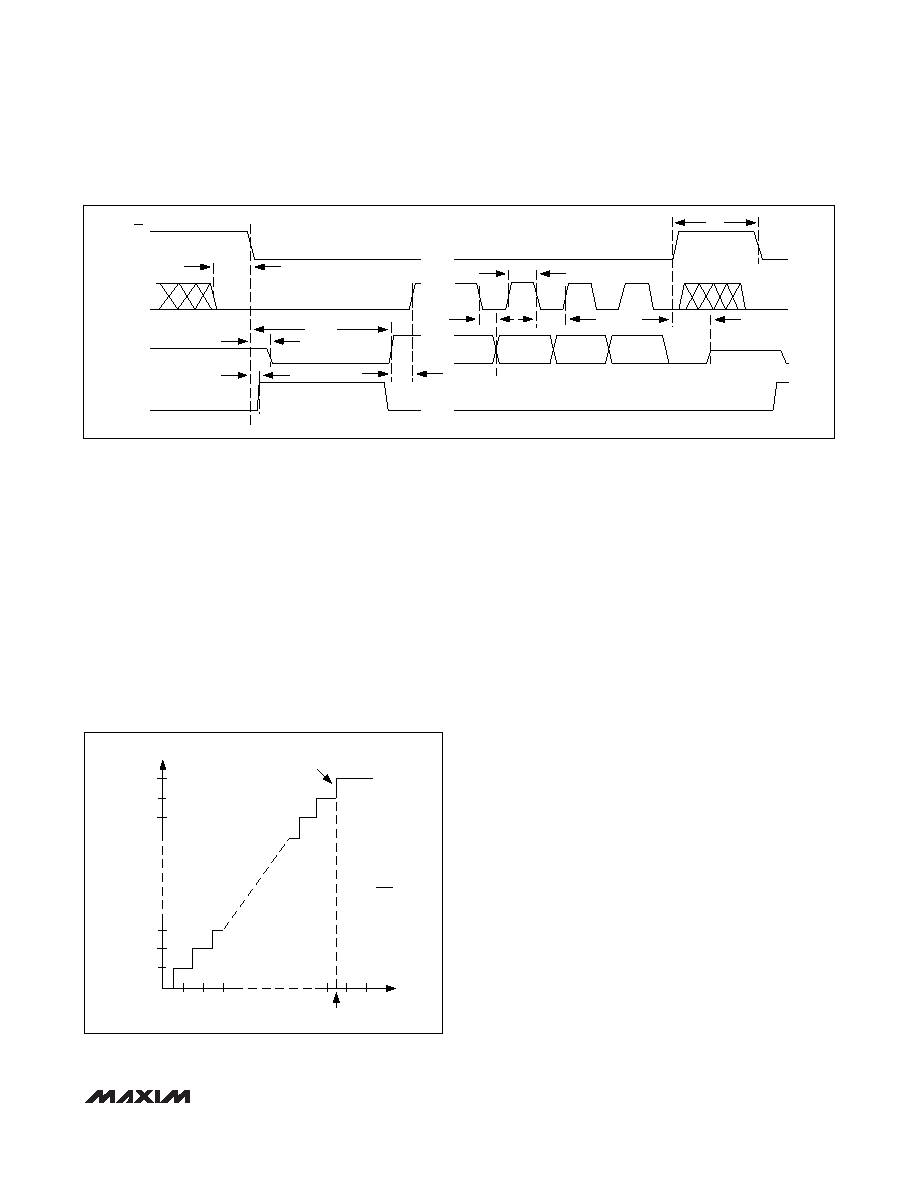
End of conversion (EOC) is signaled by DOUT going
high. DOUT’s rising edge can be used as a framing
signal. SCLK shifts the data out of this register any time
after the conversion is complete. DOUT transitions on
SCLK’s falling edge. The next falling clock edge pro-
duces the MSB of the conversion at DOUT, followed by
the remaining bits. Since there are 12 data bits and one
leading high bit, at least 13 falling clock edges are
needed to shift out these bits. Extra clock pulses occur-
ring after the conversion result has been clocked out,
and prior to a rising edge of CS, produce trailing zeros
at DOUT and have no effect on converter operation.
Minimum cycle time is accomplished by using DOUT’s
rising edge as the EOC signal. Clock out the data with
12.5 clock cycles at full speed. Pull CS high after reading
the conversion’s LSB. After the specified minimum time
(tCS), CS can be pulled low again to initiate the next
conversion.
Output Coding and Transfer Function
The data output from the MAX1240/MAX1241 is binary,
and Figure 10 depicts the nominal transfer function.
Code transitions occur halfway between successive-
integer LSB values. If VREF = +2.500V, then 1 LSB =
610V or 2.500V/4096.
____________Applications Information
Connection to Standard Interfaces
The MAX1240/MAX1241 serial interface is fully compat-
ible with SPI/QSPI and MICROWIRE standard serial
interfaces (Figure 11).
If a serial interface is available, set the CPU’s serial
interface in master mode so the CPU generates the ser-
ial clock. Choose a clock frequency up to 2.1MHz.
1) Use a general-purpose I/O line on the CPU to pull CS
low. Keep SCLK low.
2) Wait the for the maximum conversion time specified
before activating SCLK. Alternatively, look for a DOUT
rising edge to determine the end of conversion.
3) Activate SCLK for a minimum of 13 clock cycles. The
first falling clock edge produces the MSB of the
DOUT conversion. DOUT output data transitions on
SCLK’s falling edge and is available in MSB-first for-
mat. Observe the SCLK to DOUT valid timing char-
acteristic. Data can be clocked into the P on
SCLK’s rising edge.
4) Pull CS high at or after the 13th falling clock edge. If
CS remains low, trailing zeros are clocked out after
the LSB.
MAX1240/MAX1241
+2.7V, Low-Power,
12-Bit Serial ADCs in 8-Pin SO
______________________________________________________________________________________
11
11
…111
11
…110
11
…101
00
…011
00
…010
00
…001
00
…000
01
2
FS
OUTPUT CODE
FS - 3/2 LSB
INPUT VOLTAGE (LSBs)
FS = VREF - 1 LSB
1 LSB =
VREF
4096
FULL-SCALE
TRANSITION
3
…
CS
SCLK
DOUT
INTERNAL
T/H
(TRACK/ACQUIRE)
tCS0
tCONV
tDV
tAPR
tSTR
(HOLD)
(TRACK/ACQUIRE)
B2
B1
B0
tCH
tDO
tCL
tTR
tCS
Figure 10. Unipolar Transfer Function, Full Scale (FS) = VREF -
1 LSB, Zero Scale (ZS) = GND
Figure 9. Detailed Serial-Interface Timing
相关PDF资料 |
PDF描述 |
|---|---|
| MAX3241ECUI+ | IC TXRX RS-232 LP 28-TSSOP |
| MAX1027BCEE+ | IC ADC 10-BIT 300KSPS 16-QSOP |
| MAX3244ECWI+ | IC TXRX RS232 250KBPS SD 28-SOIC |
| MX7576JCWN+ | IC ADC 8BIT MPU COMP 18-SOIC |
| MAX560CAI+ | IC TXRX RS232 3.3V 28-SSOP |
相关代理商/技术参数 |
参数描述 |
|---|---|
| MAX1241CCSA+ | 功能描述:模数转换器 - ADC 12-Bit 73ksps 5.25V Precision ADC RoHS:否 制造商:Texas Instruments 通道数量:2 结构:Sigma-Delta 转换速率:125 SPs to 8 KSPs 分辨率:24 bit 输入类型:Differential 信噪比:107 dB 接口类型:SPI 工作电源电压:1.7 V to 3.6 V, 2.7 V to 5.25 V 最大工作温度:+ 85 C 安装风格:SMD/SMT 封装 / 箱体:VQFN-32 |
| MAX1241CCSA+T | 功能描述:模数转换器 - ADC 12-Bit 73ksps 5.25V Precision ADC RoHS:否 制造商:Texas Instruments 通道数量:2 结构:Sigma-Delta 转换速率:125 SPs to 8 KSPs 分辨率:24 bit 输入类型:Differential 信噪比:107 dB 接口类型:SPI 工作电源电压:1.7 V to 3.6 V, 2.7 V to 5.25 V 最大工作温度:+ 85 C 安装风格:SMD/SMT 封装 / 箱体:VQFN-32 |
| MAX1241CCSA-T | 功能描述:模数转换器 - ADC RoHS:否 制造商:Texas Instruments 通道数量:2 结构:Sigma-Delta 转换速率:125 SPs to 8 KSPs 分辨率:24 bit 输入类型:Differential 信噪比:107 dB 接口类型:SPI 工作电源电压:1.7 V to 3.6 V, 2.7 V to 5.25 V 最大工作温度:+ 85 C 安装风格:SMD/SMT 封装 / 箱体:VQFN-32 |
| MAX1241CEPA | 功能描述:模数转换器 - ADC RoHS:否 制造商:Texas Instruments 通道数量:2 结构:Sigma-Delta 转换速率:125 SPs to 8 KSPs 分辨率:24 bit 输入类型:Differential 信噪比:107 dB 接口类型:SPI 工作电源电压:1.7 V to 3.6 V, 2.7 V to 5.25 V 最大工作温度:+ 85 C 安装风格:SMD/SMT 封装 / 箱体:VQFN-32 |
| MAX1241CEPA+ | 功能描述:模数转换器 - ADC 12-Bit 73ksps 5.25V Precision ADC RoHS:否 制造商:Texas Instruments 通道数量:2 结构:Sigma-Delta 转换速率:125 SPs to 8 KSPs 分辨率:24 bit 输入类型:Differential 信噪比:107 dB 接口类型:SPI 工作电源电压:1.7 V to 3.6 V, 2.7 V to 5.25 V 最大工作温度:+ 85 C 安装风格:SMD/SMT 封装 / 箱体:VQFN-32 |
发布紧急采购,3分钟左右您将得到回复。