- 您现在的位置:买卖IC网 > PDF目录10495 > MAX1242AESA+ (Maxim Integrated Products)IC ADC 10BIT SERIAL 8-SOIC PDF资料下载
参数资料
| 型号: | MAX1242AESA+ |
| 厂商: | Maxim Integrated Products |
| 文件页数: | 10/13页 |
| 文件大小: | 0K |
| 描述: | IC ADC 10BIT SERIAL 8-SOIC |
| 产品培训模块: | Lead (SnPb) Finish for COTS Obsolescence Mitigation Program |
| 标准包装: | 100 |
| 位数: | 10 |
| 采样率(每秒): | 73k |
| 数据接口: | MICROWIRE?,QSPI?,串行,SPI? |
| 转换器数目: | 1 |
| 功率耗散(最大): | 471mW |
| 电压电源: | 单电源 |
| 工作温度: | -40°C ~ 85°C |
| 安装类型: | 表面贴装 |
| 封装/外壳: | 8-SOIC(0.154",3.90mm 宽) |
| 供应商设备封装: | 8-SOIC |
| 包装: | 管件 |
| 输入数目和类型: | 1 个单端,单极 |
MAX1242/MAX1243
+2.7V to +5.25V, Low-Power, 10-Bit
Serial ADCs in SO-8
6
Maxim Integrated
_______________Detailed Description
Converter Operation
The MAX1242/MAX1243 use an input track/hold (T/H)
and successive-approximation register (SAR) circuitry
to convert an analog input signal to a digital 10-bit out-
put. Figure 3 shows the MAX1242/MAX1243 in their
simplest configuration. The MAX1242/MAX1243 convert
input signals in the 0V to VREF range in 9s, including
T/H acquisition time. The MAX1242’s internal reference
is trimmed to 2.5V, while the MAX1243 requires an
external reference. Both devices accept external refer-
ence voltages from 1.0V to VDD. The serial interface
requires only three digital lines (SCLK, CS, and DOUT)
and provides an easy interface to microprocessors
(
μPs).
The MAX1242/MAX1243 have two modes: normal and
shutdown. Pulling SHDN low shuts the device down and
reduces supply current below 10A (VDD ≤ 3.6V), while
pulling SHDN high or leaving it open puts the devices
into operational mode. A conversion is initiated by
pulling CS low. The conversion result is available at
DOUT in unipolar serial format. The serial-data stream
consists of a high bit, signaling the end of conversion
(EOC), followed by the data bits (MSB first).
Analog Input
Figure 4 illustrates the sampling architecture of the ana-
log-to-digital converter’s (ADC’s) comparator. The full-
scale input voltage is set by the voltage at REF.
Track/Hold
In track mode, the analog signal is acquired and stored
in the internal hold capacitor. In hold mode, the T/H
switch opens and maintains a constant input to the
ADC’s SAR section.
During acquisition, the analog input AIN charges
capacitor CHOLD. Bringing CS low ends the acquisition
interval. At this instant, the T/H switches the input side
of CHOLD to GND. The retained charge on CHOLD repre-
sents a sample of the input, unbalancing node ZERO at
the comparator’s input.
In hold mode, the capacitive digital-to-analog converter
(DAC) adjusts during the remainder of the conversion
cycle to restore node ZERO to 0V within the limits of 10-
bit resolution. This action is equivalent to transferring a
charge from CHOLD to the binary-weighted capacitive
DAC, which in turn forms a digital representation of the
analog input signal. At the conversion’s end, the input
side of CHOLD switches back to AIN, and CHOLD
charges to the input signal again.
The time required for the T/H to acquire an input signal
is a function of how quickly its input capacitance is
charged. If the input signal’s source impedance is high,
the acquisition time lengthens, and more time must be
allowed between conversions. The acquisition time,
tACQ, is the maximum time the device takes to acquire
the signal and the minimum time needed for the signal
to be acquired. Acquisition time is calculated by:
tACQ = 7(RS + RIN) x 16pF
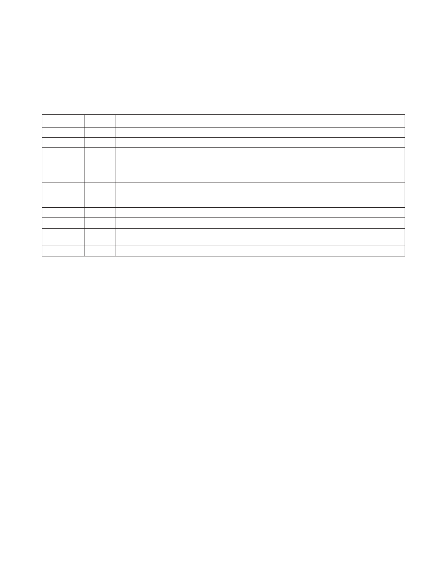
______________________________________________________________Pin Description
6
DOUT
Serial-Data Output. Data changes state at SCLK’s falling edge. High impedance when CS is high.
8
SCLK
3
SHDN
Three-Level Shutdown Input. Pulling SHDN low shuts the MAX1242/MAX1243 down to 15A (max)
supply current. Both MAX1242 and MAX1243 are fully operational with either SHDN high or open. For
the MAX1242, pulling SHDN high enables the internal reference, and letting SHDN open disables the
internal reference and allows for the use of an external reference.
4
REF
Reference Voltage for Analog-to-Digital Conversion. Internal 2.5V reference output for MAX1242;
bypass with a 4.7F capacitor. External reference voltage input for MAX1243, or for MAX1242 with the
internal reference disabled. Bypass REF with a minimum of 0.1F when using an external reference.
7
CS
Active-Low Chip Select. Initiates conversions on the falling edge. When CS is high, DOUT is high
impedance.
5
GND
Analog and Digital Ground
2
AIN
Sampling Analog Input, 0V to VREF range
NAME
FUNCTION
1
VDD
Positive Supply Voltage: +2.7V to +5.25V
PIN
Serial-Clock Input. SCLK clocks data out at rates up to 2.1MHz.
相关PDF资料 |
PDF描述 |
|---|---|
| MAX1084BESA+ | IC ADC 10BIT 400KSPS 8-SOIC |
| MAX1241ACSA+ | IC ADC SRL 12BIT 2.7V 8-SOIC |
| VI-B53-IV-F4 | CONVERTER MOD DC/DC 24V 150W |
| MAX147BCPP+ | IC SRL ADC 8CH 12BIT 2.7V 20-DIP |
| MAX213EEWI+ | IC TXRX RS-232 W/CAP 28-SOIC |
相关代理商/技术参数 |
参数描述 |
|---|---|
| MAX1242AESA+ | 功能描述:模数转换器 - ADC 10-Bit 73ksps 5.25V Precision ADC RoHS:否 制造商:Texas Instruments 通道数量:2 结构:Sigma-Delta 转换速率:125 SPs to 8 KSPs 分辨率:24 bit 输入类型:Differential 信噪比:107 dB 接口类型:SPI 工作电源电压:1.7 V to 3.6 V, 2.7 V to 5.25 V 最大工作温度:+ 85 C 安装风格:SMD/SMT 封装 / 箱体:VQFN-32 |
| MAX1242AESA+T | 功能描述:模数转换器 - ADC 10-Bit 73ksps 5.25V Precision ADC RoHS:否 制造商:Texas Instruments 通道数量:2 结构:Sigma-Delta 转换速率:125 SPs to 8 KSPs 分辨率:24 bit 输入类型:Differential 信噪比:107 dB 接口类型:SPI 工作电源电压:1.7 V to 3.6 V, 2.7 V to 5.25 V 最大工作温度:+ 85 C 安装风格:SMD/SMT 封装 / 箱体:VQFN-32 |
| MAX1242AESA-T | 功能描述:模数转换器 - ADC RoHS:否 制造商:Texas Instruments 通道数量:2 结构:Sigma-Delta 转换速率:125 SPs to 8 KSPs 分辨率:24 bit 输入类型:Differential 信噪比:107 dB 接口类型:SPI 工作电源电压:1.7 V to 3.6 V, 2.7 V to 5.25 V 最大工作温度:+ 85 C 安装风格:SMD/SMT 封装 / 箱体:VQFN-32 |
| MAX1242AMJA | 功能描述:模数转换器 - ADC RoHS:否 制造商:Texas Instruments 通道数量:2 结构:Sigma-Delta 转换速率:125 SPs to 8 KSPs 分辨率:24 bit 输入类型:Differential 信噪比:107 dB 接口类型:SPI 工作电源电压:1.7 V to 3.6 V, 2.7 V to 5.25 V 最大工作温度:+ 85 C 安装风格:SMD/SMT 封装 / 箱体:VQFN-32 |
| MAX1242BCPA | 功能描述:模数转换器 - ADC Integrated Circuits (ICs) RoHS:否 制造商:Texas Instruments 通道数量:2 结构:Sigma-Delta 转换速率:125 SPs to 8 KSPs 分辨率:24 bit 输入类型:Differential 信噪比:107 dB 接口类型:SPI 工作电源电压:1.7 V to 3.6 V, 2.7 V to 5.25 V 最大工作温度:+ 85 C 安装风格:SMD/SMT 封装 / 箱体:VQFN-32 |
发布紧急采购,3分钟左右您将得到回复。