- 您现在的位置:买卖IC网 > PDF目录383316 > MAX1247AEEE (MAXIM INTEGRATED PRODUCTS INC) LJT 10C 10#20 SKT RECP PDF资料下载
参数资料
| 型号: | MAX1247AEEE |
| 厂商: | MAXIM INTEGRATED PRODUCTS INC |
| 元件分类: | ADC |
| 英文描述: | LJT 10C 10#20 SKT RECP |
| 中文描述: | 4-CH 12-BIT SUCCESSIVE APPROXIMATION ADC, SERIAL ACCESS, PDSO16 |
| 封装: | 0.150 INCH, 0.025 INCH PITCH, QSOP-16 |
| 文件页数: | 9/24页 |
| 文件大小: | 223K |
| 代理商: | MAX1247AEEE |
M
+2.7V, Low-Power, 4-Channel,
S erial 12-Bit ADCs in QS OP-16
_______________________________________________________________________________________
9
_______________Detailed Desc ription
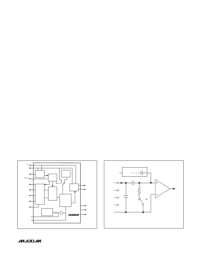
The MAX1246/MAX1247 analog-to-digital converters
(ADCs) use a successive-approximation conversion
technique and input track/hold (T/H) circuitry to convert
an analog signal to a 12-bit digital output. A flexible seri-
al interface provides easy interface to microprocessors
(μPs). Figure 3 is a block diagram of the MAX1246/
MAX1247.
Pseudo-Differential Input
The sampling architecture of the ADC’s analog com-
parator is illustrated in the equivalent input circuit
(Figure 4). In single-ended mode, IN+ is internally
switched to CH0–CH3, and IN- is switched to COM. In
differential mode, IN+ and IN- are selected from two
pairs: CH0/CH1 and CH2/CH3. Configure the channels
with Tables 2 and 3. Please note that the codes for
CH0–CH3 in the MAX1246/MAX1247 correspond to the
codes for CH2–CH5 in the eight-channel (MAX146/
MAX147) versions.
In differential mode, IN- and IN+ are internally switched
to either of the analog inputs. This configuration is
pseudo-differential to the effect that only the signal at IN+
is sampled. The return side (IN-) must remain stable within
±0.5LSB (±0.1LSB for best results) with respect to AGND
during a conversion. To accomplish this, connect a 0.1μF
capacitor from IN- (the selected analog input) to AGND.
During the acquisition interval, the channel selected
as the positive input (IN+) charges capacitor C
HOLD
.
The acquisition interval spans three SCLK cycles and
ends on the falling SCLK edge after the last bit of the
input control word has been entered. At the end of the
acquisition interval, the T/H switch opens, retaining
charge on C
HOLD
as a sample of the signal at IN+.
The conversion interval begins with the input multiplexer
switching C
HOLD
from the positive input (IN+) to the
negative input (IN-). In single-ended mode, IN- is simply
COM. This unbalances node ZERO at the comparator’s
input. The capacitive DAC adjusts during the remainder
of the conversion cycle to restore node ZERO to 0V
within the limits of 12-bit resolution. This action is equiv-
alent to transferring a 16pF x [(V
IN
+
) - (V
IN
-)] charge
from C
HOLD
to the binary-weighted capacitive DAC,
which in turn forms a digital representation of the analog
input signal.
T rac k/Hold
The T/H enters its tracking mode on the falling clock
edge after the fifth bit of the 8-bit control word has been
shifted in. It enters its hold mode on the falling clock
edge after the eighth bit of the control word has been
shifted in. If the converter is set up for single-ended
inputs, IN- is connected to COM, and the converter
samples the “+” input. If the converter is set up for dif-
ferential inputs, IN- connects to the “-” input, and the
difference of
|
IN+ - IN-
|
is sampled. At the end of the
conversion, the positive input connects back to IN+,
and C
HOLD
charges to the input signal.
The time required for the T/H to acquire an input signal
is a function of how quickly its input capacitance is
charged. If the input signal’s source impedance is high,
the acquisition time lengthens, and more time must be
INPUT
SHIFT
REGISTER
CONTROL
LOGIC
INT
CLOCK
OUTPUT
SHIFT
REGISTER
+1.21V
REFERENCE
(MAX1246)
T/H
ANALOG
INPUT
MUX
12-BIT
SAR
ADC
REF
IN
DOUT
SSTRB
V
DD
DGND
AGND
SCLK
DIN
COM
REFADJ
VREF
OUT
CLOCK
+2.500V
20k
*A
≈
2.00 (MAX1247)
7
8
9
6
12
13
14
15
16
CH3
5
CH2
4
CH1
3
CH0
2
MAX1246
MAX1247
CS
SHDN
1
11
10
≈
2.06*
A
Figure 3. Block Diagram
CH0
CH1
CH2
CH3
COM
C
SWITCH
TRACK
T/H
SWITCH
R
IN
9k
C
HOLD
HOLD
12-BIT CAPACITIVE DAC
VREF
ZERO
COMPARATOR
–
+
16pF
SINGLE-ENDED MODE: IN+ = CH0–CH3, IN- = COM.
DIFFERENTIAL MODE: IN+ AND IN- SELECTED FROM PAIRS OF
CH0/CH1 AND CH2/CH3.
AT THE SAMPLING INSTANT,
THE MUX INPUT SWITCHES
FROM THE SELECTED IN+
CHANNEL TOTHE SELECTED
IN- CHANNEL.
INPUT
MUX
Figure 4. Equivalent Input Circuit
相关PDF资料 |
PDF描述 |
|---|---|
| MAX1246ACPE | 0.1UF 5% 50VDC (1912) PPS FILM CAP |
| MAX1246AEPE | +2.7V, Low-Power, 4-Channel, Serial 12-Bit ADCs in QSOP-16 |
| MAX1246AMJE | +2.7V, Low-Power, 4-Channel, Serial 12-Bit ADCs in QSOP-16 |
| MAX1246BCEE | +2.7V, Low-Power, 4-Channel, Serial 12-Bit ADCs in QSOP-16 |
| MAX1246BCPE | +2.7V, Low-Power, 4-Channel, Serial 12-Bit ADCs in QSOP-16 |
相关代理商/技术参数 |
参数描述 |
|---|---|
| MAX1247AEEE+ | 功能描述:模数转换器 - ADC 12-Bit 4Ch 133ksps 5.25V Precision ADC RoHS:否 制造商:Texas Instruments 通道数量:2 结构:Sigma-Delta 转换速率:125 SPs to 8 KSPs 分辨率:24 bit 输入类型:Differential 信噪比:107 dB 接口类型:SPI 工作电源电压:1.7 V to 3.6 V, 2.7 V to 5.25 V 最大工作温度:+ 85 C 安装风格:SMD/SMT 封装 / 箱体:VQFN-32 |
| MAX1247AEEE+T | 功能描述:模数转换器 - ADC 12-Bit 4Ch 133ksps 5.25V Precision ADC RoHS:否 制造商:Texas Instruments 通道数量:2 结构:Sigma-Delta 转换速率:125 SPs to 8 KSPs 分辨率:24 bit 输入类型:Differential 信噪比:107 dB 接口类型:SPI 工作电源电压:1.7 V to 3.6 V, 2.7 V to 5.25 V 最大工作温度:+ 85 C 安装风格:SMD/SMT 封装 / 箱体:VQFN-32 |
| MAX1247AEEE-T | 功能描述:模数转换器 - ADC RoHS:否 制造商:Texas Instruments 通道数量:2 结构:Sigma-Delta 转换速率:125 SPs to 8 KSPs 分辨率:24 bit 输入类型:Differential 信噪比:107 dB 接口类型:SPI 工作电源电压:1.7 V to 3.6 V, 2.7 V to 5.25 V 最大工作温度:+ 85 C 安装风格:SMD/SMT 封装 / 箱体:VQFN-32 |
| MAX1247AEPE | 功能描述:模数转换器 - ADC Integrated Circuits (ICs) RoHS:否 制造商:Texas Instruments 通道数量:2 结构:Sigma-Delta 转换速率:125 SPs to 8 KSPs 分辨率:24 bit 输入类型:Differential 信噪比:107 dB 接口类型:SPI 工作电源电压:1.7 V to 3.6 V, 2.7 V to 5.25 V 最大工作温度:+ 85 C 安装风格:SMD/SMT 封装 / 箱体:VQFN-32 |
| MAX1247AEPE+ | 功能描述:模数转换器 - ADC 12-Bit 4Ch 133ksps 5.25V Precision ADC RoHS:否 制造商:Texas Instruments 通道数量:2 结构:Sigma-Delta 转换速率:125 SPs to 8 KSPs 分辨率:24 bit 输入类型:Differential 信噪比:107 dB 接口类型:SPI 工作电源电压:1.7 V to 3.6 V, 2.7 V to 5.25 V 最大工作温度:+ 85 C 安装风格:SMD/SMT 封装 / 箱体:VQFN-32 |
发布紧急采购,3分钟左右您将得到回复。