- 您现在的位置:买卖IC网 > PDF目录9871 > MAX1247BEPE+ (Maxim Integrated Products)IC ADC 12BIT SERIAL 16-DIP PDF资料下载
参数资料
| 型号: | MAX1247BEPE+ |
| 厂商: | Maxim Integrated Products |
| 文件页数: | 12/25页 |
| 文件大小: | 0K |
| 描述: | IC ADC 12BIT SERIAL 16-DIP |
| 产品培训模块: | Lead (SnPb) Finish for COTS Obsolescence Mitigation Program |
| 标准包装: | 25 |
| 位数: | 12 |
| 采样率(每秒): | 133k |
| 数据接口: | MICROWIRE?,QSPI?,串行,SPI? |
| 转换器数目: | 1 |
| 功率耗散(最大): | 842mW |
| 电压电源: | 单电源 |
| 工作温度: | -40°C ~ 85°C |
| 安装类型: | 通孔 |
| 封装/外壳: | 16-DIP(0.300",7.62mm) |
| 供应商设备封装: | 16-PDIP |
| 包装: | 管件 |
| 输入数目和类型: | 4 个单端,单极;4 个单端,双极;2 个差分,单极;2 个差分,双极 |
MAX1246/MAX1247
+2.7V, Low-Power, 4-Channel,
Serial 12-Bit ADCs in QSOP-16
2
_______________________________________________________________________________________
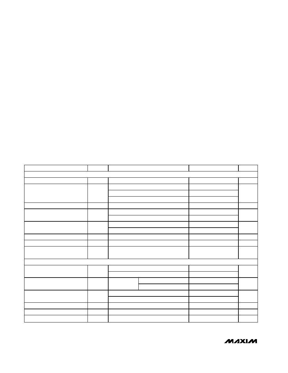
ABSOLUTE MAXIMUM RATINGS
ELECTRICAL CHARACTERISTICS
(VDD = +2.7V to +3.6V (MAX1246); VDD = +2.7V to +5.25V (MAX1247); COM = 0V; fSCLK = 2.0MHz; external clock (50% duty cycle);
15 clocks/conversion cycle (133ksps); MAX1246—4.7F capacitor at VREF pin; MAX1247—external reference, VREF = 2.5V applied
to VREF pin; TA = TMIN to TMAX; unless otherwise noted.)
Stresses beyond those listed under “Absolute Maximum Ratings” may cause permanent damage to the device. These are stress ratings only, and functional
operation of the device at these or any other conditions beyond those indicated in the operational sections of the specifications is not implied. Exposure to
absolute maximum rating conditions for extended periods may affect device reliability.
VDD to AGND, DGND................................................. -0.3V to 6V
AGND to DGND ...................................................... -0.3V to 0.3V
CH0–CH3, COM to AGND, DGND ............ -0.3V to (VDD + 0.3V)
VREF to AGND........................................... -0.3V to (VDD + 0.3V)
Digital Inputs to DGND .............................................. -0.3V to 6V
Digital Outputs to DGND ........................... -0.3V to (VDD + 0.3V)
Digital Output Sink Current .................................................25mA
Continuous Power Dissipation (TA = +70°C)
Plastic DIP (derate 10.53mW/°C above +70°C) ......... 842mW
QSOP (derate 8.36mW/°C above +70°C) ................... 667mW
CERDIP (derate 10.00mW/°C above +70°C) .............. 800mW
Operating Temperature Ranges
MAX1246_C_E/MAX1247_C_E .......................... 0°C to +70°C
MAX1246_E_E/MAX1247_E_E........................ -40°C to +85°C
MAX1246_MJE/MAX1247_MJE .................... -55°C to +125°C
Storage Temperature Range ............................ -60°C to +150°C
Lead Temperature (soldering, 10s) ................................ +300°C
PARAMETER
SYMBOL
CONDITIONS
MIN
TYP
MAX
UNITS
DC ACCURACY (Note 1)
Resolution
12
Bits
MAX124_A
±0.5
MAX124_B
±1.0
Relative Accuracy (Note 2)
INL
MAX1247C
±2.0
LSB
No Missing Codes
NMC
12
Bits
MAX124_A/MAX124_B
±1
Differential Nonlinearity
DNL
MAX124_C
±0.8
LSB
MAX124_A
±0.5
±3
Offset Error
MAX124_B
±0.5
±4
LSB
Gain Error (Note 3)
±0.5
±4
LSB
Gain Temperature Coefficient
±0.25
ppm/°C
Channel-to-Channel Offset
Matching
±0.25
LSB
DYNAMIC SPECIFICATIONS (10kHz sine-wave input, 0V to 2.500Vp-p, 133ksps, 2.0MHz external clock, bipolar input mode)
MAX124_A/MAX124_B
70
73
Signal-to-Noise + Distortion
Ratio
SINAD
MAX1247C
73
dB
MAX124_A/MAX124_B
-88
-80
Total Harmonic Distortion
THD
Up to the 5th
harmonic
MAX1247C
-88
dB
MAX124_A/MAX124_B
80
90
Spurious-Free Dynamic Range
SFDR
MAX1247C
90
dB
Channel-to-Channel Crosstalk
65kHz, 2.500VP-P (Note 4)
-85
dB
Small-Signal Bandwidth
-3dB rolloff
2.25
MHz
Full-Power Bandwidth
1.0
MHz
相关PDF资料 |
PDF描述 |
|---|---|
| MS27484E18B35S | CONN PLUG 66POS STRAIGHT W/SCKT |
| MS27467T15B15P | CONN PLUG 15POS STRAIGHT W/PINS |
| MS27467E15B15P | CONN PLUG 15POS STRAIGHT W/PINS |
| MS27467T15B18SC | CONN PLUG 18POS STRAIGHT W/SCKT |
| VE-27K-MX-F2 | CONVERTER MOD DC/DC 40V 75W |
相关代理商/技术参数 |
参数描述 |
|---|---|
| MAX1247BEPE+ | 功能描述:模数转换器 - ADC 12-Bit 4Ch 133ksps 5.25V Precision ADC RoHS:否 制造商:Texas Instruments 通道数量:2 结构:Sigma-Delta 转换速率:125 SPs to 8 KSPs 分辨率:24 bit 输入类型:Differential 信噪比:107 dB 接口类型:SPI 工作电源电压:1.7 V to 3.6 V, 2.7 V to 5.25 V 最大工作温度:+ 85 C 安装风格:SMD/SMT 封装 / 箱体:VQFN-32 |
| MAX1247BMEE/PR | 制造商:Maxim Integrated Products 功能描述:- Rail/Tube |
| MAX1247BMJE | 功能描述:模数转换器 - ADC RoHS:否 制造商:Texas Instruments 通道数量:2 结构:Sigma-Delta 转换速率:125 SPs to 8 KSPs 分辨率:24 bit 输入类型:Differential 信噪比:107 dB 接口类型:SPI 工作电源电压:1.7 V to 3.6 V, 2.7 V to 5.25 V 最大工作温度:+ 85 C 安装风格:SMD/SMT 封装 / 箱体:VQFN-32 |
| MAX1247CCEE | 制造商:Rochester Electronics LLC 功能描述: 制造商:Maxim Integrated Products 功能描述: |
| MAX1247CCPE | 制造商:Rochester Electronics LLC 功能描述: 制造商:Maxim Integrated Products 功能描述: |
发布紧急采购,3分钟左右您将得到回复。