- 您现在的位置:买卖IC网 > PDF目录9867 > MAX1265ACEI+ (Maxim Integrated Products)IC ADC 12BIT 265KSPS 28-QSOP PDF资料下载
参数资料
| 型号: | MAX1265ACEI+ |
| 厂商: | Maxim Integrated Products |
| 文件页数: | 8/19页 |
| 文件大小: | 0K |
| 描述: | IC ADC 12BIT 265KSPS 28-QSOP |
| 产品培训模块: | Lead (SnPb) Finish for COTS Obsolescence Mitigation Program |
| 标准包装: | 50 |
| 位数: | 12 |
| 采样率(每秒): | 265k |
| 数据接口: | 并联 |
| 转换器数目: | 1 |
| 功率耗散(最大): | 5.4mW |
| 电压电源: | 单电源 |
| 工作温度: | 0°C ~ 70°C |
| 安装类型: | 表面贴装 |
| 封装/外壳: | 28-SSOP(0.154",3.90mm 宽) |
| 供应商设备封装: | 28-QSOP |
| 包装: | 管件 |
| 输入数目和类型: | 6 个单端,单极;6 个单端,双极;3 个伪差分,单极;3 个伪差分,双极 |
MAX1265/MAX1267
265ksps, +3V, 6-/2-Channel, 12-Bit ADCs
with +2.5V Reference and Parallel Interface
16
______________________________________________________________________________________
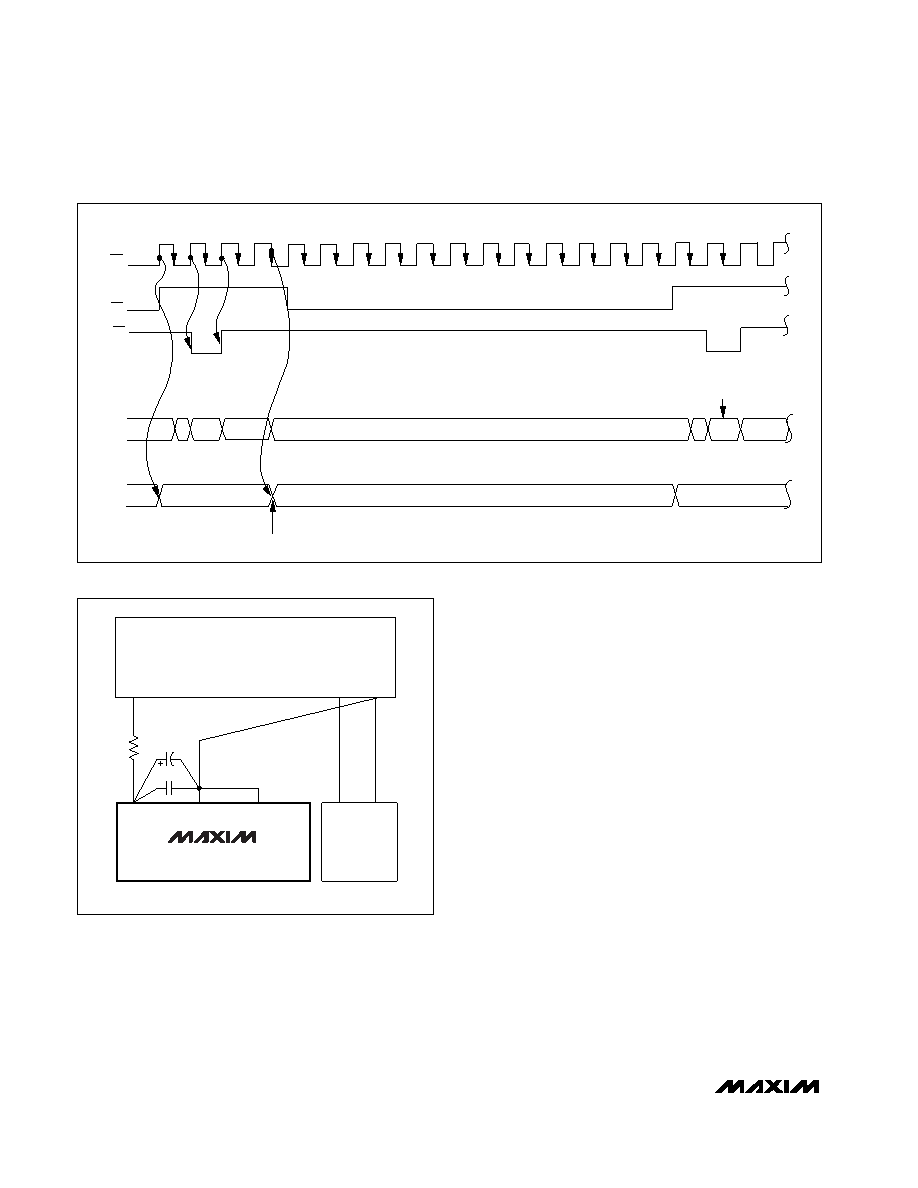
acquisition cycle of the next conversion, then reading the
results of the previous conversion from the bus. This
technique (Figure 10) allows a conversion to be com-
pleted every 16 clock cycles. Note that the switching of
the data bus during acquisition or conversion can
cause additional supply noise, which can make it diffi-
cult to achieve true 12-bit performance.
Layout, Grounding, and Bypassing
For best performance, use printed circuit (PC) boards.
Wire-wrap configurations are not recommended since
the layout should ensure proper separation of analog
and digital traces. Do not run analog and digital lines
parallel to each other, and do not lay out digital signal
paths underneath the ADC package. Use separate
analog and digital PC board ground sections with only
one star point (Figure 11) connecting the two ground
systems (analog and digital). For lowest noise opera-
tion, ensure the ground return to the star ground’s
power supply is low impedance and as short as possi-
ble. Route digital signals far away from sensitive analog
and reference inputs.
High-frequency noise in the power supply, VDD, could
impair operation of the ADC’s fast comparator. Bypass
VDD to the star ground with a network of two parallel
capacitors, 0.1F and 4.7F, located as close as to the
MAX1265/MAX1267s’ power-supply pin as possible.
Minimize capacitor lead length for best supply-noise
rejection and add an attenuation resistor (5
) if the
power supply is extremely noisy.
Figure 11. Power-Supply and Grounding Connections
Figure 10. Timing Diagram for Fastest Conversion
+3V
GND
SUPPLIES
DGND
+3V
COM
GND
4.7
F
0.1
F
VDD
DIGITAL
CIRCUITRY
MAX1265
MAX1267
*R = 5
*OPTIONAL
CLK
ACQUISITION
CONTROL WORD
CONVERSION
D11–D0
ACQUISITION
SAMPLING INSTANT
12
3
4
5
6
7
8
9
10
11
12
13
14
15
16
WR
RD
D7–D0
STATE
;
CONTROL
WORD
D11–
D0
相关PDF资料 |
PDF描述 |
|---|---|
| VE-2TP-MX-F4 | CONVERTER MOD DC/DC 13.8V 75W |
| VE-2TP-MX-F3 | CONVERTER MOD DC/DC 13.8V 75W |
| VE-2TP-MX-F2 | CONVERTER MOD DC/DC 13.8V 75W |
| MS27468T15B35P EDR | CONN RCPT 37POS JAM NUT W/PINS |
| ISL59911IRZ-T7 | IC RCVR/EQUALZR TRPL DIFF 32QFN |
相关代理商/技术参数 |
参数描述 |
|---|---|
| MAX1265ACEI+ | 功能描述:模数转换器 - ADC 12-Bit 6Ch 265ksps 3.6V Precision ADC RoHS:否 制造商:Texas Instruments 通道数量:2 结构:Sigma-Delta 转换速率:125 SPs to 8 KSPs 分辨率:24 bit 输入类型:Differential 信噪比:107 dB 接口类型:SPI 工作电源电压:1.7 V to 3.6 V, 2.7 V to 5.25 V 最大工作温度:+ 85 C 安装风格:SMD/SMT 封装 / 箱体:VQFN-32 |
| MAX1265ACEI+T | 功能描述:模数转换器 - ADC 12-Bit 6Ch 265ksps 3.6V Precision ADC RoHS:否 制造商:Texas Instruments 通道数量:2 结构:Sigma-Delta 转换速率:125 SPs to 8 KSPs 分辨率:24 bit 输入类型:Differential 信噪比:107 dB 接口类型:SPI 工作电源电压:1.7 V to 3.6 V, 2.7 V to 5.25 V 最大工作温度:+ 85 C 安装风格:SMD/SMT 封装 / 箱体:VQFN-32 |
| MAX1265ACEI-T | 功能描述:模数转换器 - ADC RoHS:否 制造商:Texas Instruments 通道数量:2 结构:Sigma-Delta 转换速率:125 SPs to 8 KSPs 分辨率:24 bit 输入类型:Differential 信噪比:107 dB 接口类型:SPI 工作电源电压:1.7 V to 3.6 V, 2.7 V to 5.25 V 最大工作温度:+ 85 C 安装风格:SMD/SMT 封装 / 箱体:VQFN-32 |
| MAX1265AEEI | 功能描述:模数转换器 - ADC RoHS:否 制造商:Texas Instruments 通道数量:2 结构:Sigma-Delta 转换速率:125 SPs to 8 KSPs 分辨率:24 bit 输入类型:Differential 信噪比:107 dB 接口类型:SPI 工作电源电压:1.7 V to 3.6 V, 2.7 V to 5.25 V 最大工作温度:+ 85 C 安装风格:SMD/SMT 封装 / 箱体:VQFN-32 |
| MAX1265AEEI+ | 功能描述:模数转换器 - ADC 12-Bit 6Ch 265ksps 3.6V Precision ADC RoHS:否 制造商:Texas Instruments 通道数量:2 结构:Sigma-Delta 转换速率:125 SPs to 8 KSPs 分辨率:24 bit 输入类型:Differential 信噪比:107 dB 接口类型:SPI 工作电源电压:1.7 V to 3.6 V, 2.7 V to 5.25 V 最大工作温度:+ 85 C 安装风格:SMD/SMT 封装 / 箱体:VQFN-32 |
发布紧急采购,3分钟左右您将得到回复。