- 您现在的位置:买卖IC网 > PDF目录17009 > MAX1270EVKIT (Maxim Integrated Products)EVALUATION KIT FOR MAX1270 PDF资料下载
参数资料
| 型号: | MAX1270EVKIT |
| 厂商: | Maxim Integrated Products |
| 文件页数: | 5/20页 |
| 文件大小: | 0K |
| 描述: | EVALUATION KIT FOR MAX1270 |
| 产品培训模块: | Lead (SnPb) Finish for COTS Obsolescence Mitigation Program |
| 标准包装: | 1 |
| ADC 的数量: | 1 |
| 位数: | 12 |
| 采样率(每秒): | 110k |
| 数据接口: | 串行 |
| 输入范围: | ±10 V |
| 在以下条件下的电源(标准): | 30mW @ 110kSPS |
| 工作温度: | 0°C ~ 70°C |
| 已用 IC / 零件: | MAX1270,MAX1271,MAX127,MAX128 |
| 已供物品: | 板,CD |
MAX1270/MAX1271
Multirange, +5V, 8-Channel,
Serial 12-Bit ADCs
______________________________________________________________________________________
13
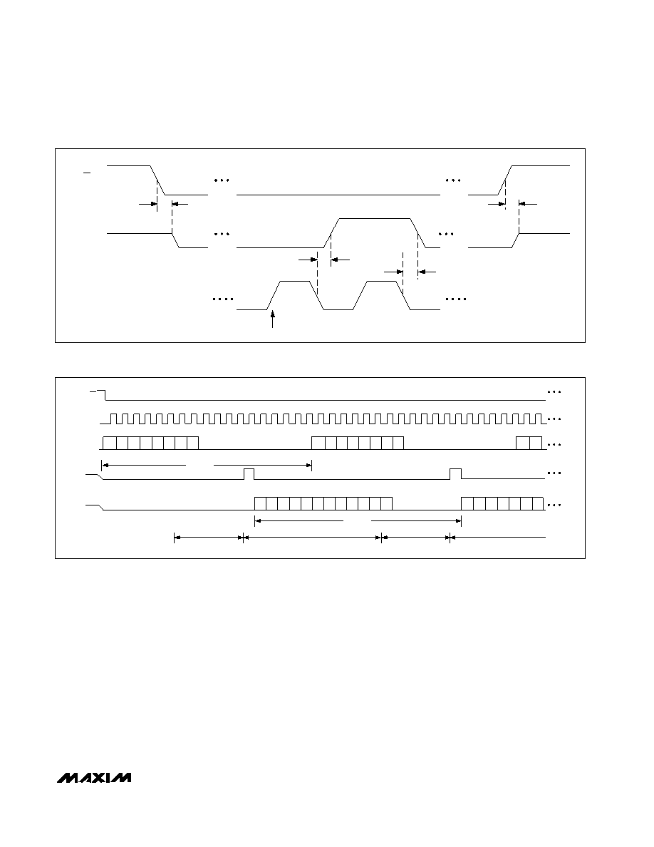
Internal Clock Mode (PD1 = 0, PD0 = 0)
In internal clock mode, the MAX1270/MAX1271 gener-
ate their conversion clock internally. This frees the
microprocessor from the burden of running the acquisi-
tion and the SAR conversion clock, and allows the con-
version results to be read back at the processor’s
convenience, at any clock rate from 0 to typically
10MHz.
SSTRB goes low after the falling edge of the last bit
(PD0) of the control byte has been shifted in, and
returns high when the conversion is complete.
Acquisition is completed and conversion begins on the
falling edge of the 4th internal clock pulse after the con-
trol byte; conversion ends on the falling edge of the
16th internal clock pulse (12 internal clock cycle pulses
are used for conversion). SSTRB will remain low for a
maximum of 15s, during which time SCLK should
remain low for best noise performance. An internal reg-
ister stores data while the conversion is in progress.
The MSB of the result byte (D11) is present at DOUT
starting at the falling edge of the last internal clock of
conversion. Successive falling edges of SCLK will shift
the remaining data out of this register (Figure 9).
Additional SCLK edges will result in zeros on DOUT.
When internal clock mode is selected, SSTRB does not
go into a high-impedance state when CS goes high.
Pulling CS high prevents data from being clocked in
and tri-states DOUT, but does not adversely affect a
tSDV
tSSTRB
SCLK 12
tSTR
SSTRB
SCLK
CS
tSSTRB
HIGH-Z
Figure 7. External Clock Mode—SSTRB Detailed Timing
CS
SCLK
DIN
DOUT
A/D STATE
13
19
24
26
31
32
14
16
37
START SEL2 SEL1 SEL0
BIP
RNG
PD1 PD0
D11 D10
D9
D7
D8
D6
D5
D4
D2
D3
D1
D0
LSB
8
1
MSB
LSB
MSB
START SEL2 SEL1 SEL0
BIP
RNG
PD1 PD0
START SEL2
CONTROL BYTE 0
RESULT
CONTROL BYTE 1
CONTROL BYTE 2
18 SCLK
SSTRB
D10
D11
D9
D8
D6
D7
D5
RESULT 1
ACQUISITION
6 SCLK
CONVERSION
12 SCLK
ACQUISITION
6 SCLK
CONVERSION
12 SCLK
HIGH-Z
Figure 8. External Clock Mode—18 Clocks/Conversion Timing
相关PDF资料 |
PDF描述 |
|---|---|
| VE-JWH-EY | CONVERTER MOD DC/DC 52V 50W |
| 0982660145 | CBL 14POS 0.5MM JMPR TYPE A 4" |
| PCM18XQ0 | MODULE PROCESSOR FOR MPLABICE |
| HSC08DRTI | CONN EDGECARD 16POS DIP .100 SLD |
| HSC08DREI | CONN EDGECARD 16POS .100 EYELET |
相关代理商/技术参数 |
参数描述 |
|---|---|
| MAX1270EVKIT+ | 功能描述:数据转换 IC 开发工具 MAX1270/71 MAX127/8 Eval System RoHS:否 制造商:Texas Instruments 产品:Demonstration Kits 类型:ADC 工具用于评估:ADS130E08 接口类型:SPI 工作电源电压:- 6 V to + 6 V |
| MAX1271ACAI | 功能描述:模数转换器 - ADC RoHS:否 制造商:Texas Instruments 通道数量:2 结构:Sigma-Delta 转换速率:125 SPs to 8 KSPs 分辨率:24 bit 输入类型:Differential 信噪比:107 dB 接口类型:SPI 工作电源电压:1.7 V to 3.6 V, 2.7 V to 5.25 V 最大工作温度:+ 85 C 安装风格:SMD/SMT 封装 / 箱体:VQFN-32 |
| MAX1271ACAI+ | 功能描述:模数转换器 - ADC 12-Bit 8Ch 110ksps 4.18V Precision ADC RoHS:否 制造商:Texas Instruments 通道数量:2 结构:Sigma-Delta 转换速率:125 SPs to 8 KSPs 分辨率:24 bit 输入类型:Differential 信噪比:107 dB 接口类型:SPI 工作电源电压:1.7 V to 3.6 V, 2.7 V to 5.25 V 最大工作温度:+ 85 C 安装风格:SMD/SMT 封装 / 箱体:VQFN-32 |
| MAX1271ACAI+T | 功能描述:模数转换器 - ADC 12-Bit 8Ch 110ksps 4.18V Precision ADC RoHS:否 制造商:Texas Instruments 通道数量:2 结构:Sigma-Delta 转换速率:125 SPs to 8 KSPs 分辨率:24 bit 输入类型:Differential 信噪比:107 dB 接口类型:SPI 工作电源电压:1.7 V to 3.6 V, 2.7 V to 5.25 V 最大工作温度:+ 85 C 安装风格:SMD/SMT 封装 / 箱体:VQFN-32 |
| MAX1271ACAI-T | 功能描述:模数转换器 - ADC RoHS:否 制造商:Texas Instruments 通道数量:2 结构:Sigma-Delta 转换速率:125 SPs to 8 KSPs 分辨率:24 bit 输入类型:Differential 信噪比:107 dB 接口类型:SPI 工作电源电压:1.7 V to 3.6 V, 2.7 V to 5.25 V 最大工作温度:+ 85 C 安装风格:SMD/SMT 封装 / 箱体:VQFN-32 |
发布紧急采购,3分钟左右您将得到回复。