- 您现在的位置:买卖IC网 > PDF目录9917 > MAX1279AETC+T (Maxim Integrated Products)IC ADC 12BIT 1.5MSPS 12-TQFN PDF资料下载
参数资料
| 型号: | MAX1279AETC+T |
| 厂商: | Maxim Integrated Products |
| 文件页数: | 3/18页 |
| 文件大小: | 0K |
| 描述: | IC ADC 12BIT 1.5MSPS 12-TQFN |
| 产品培训模块: | Lead (SnPb) Finish for COTS Obsolescence Mitigation Program |
| 标准包装: | 2,500 |
| 位数: | 12 |
| 采样率(每秒): | 1.5M |
| 数据接口: | MICROWIRE?,QSPI?,串行,SPI? |
| 转换器数目: | 1 |
| 功率耗散(最大): | 1.35W |
| 电压电源: | 模拟和数字 |
| 工作温度: | -40°C ~ 85°C |
| 安装类型: | 表面贴装 |
| 封装/外壳: | 12-WQFN 裸露焊盘 |
| 供应商设备封装: | 12-TQFN-EP(4x4) |
| 包装: | 带卷 (TR) |
| 输入数目和类型: | 1 个差分,双极 |
Timing and Control
Conversion-start and data-read operations are con-
trolled by the CNVST and SCLK digital inputs. Figures 1
and 5 show timing diagrams, which outline the serial-
interface operation.
A CNVST falling edge initiates a conversion sequence;
the T/H stage holds the input voltage, the ADC begins
to convert, and DOUT changes from high impedance to
logic low. SCLK is used to drive the conversion
process, and it shifts data out as each bit of the conver-
sion is determined.
SCLK begins shifting out the data after the 4th rising
edge of SCLK. DOUT transitions tDOUT after each
SCLK’s rising edge and remains valid 4ns (tDHOLD)
after the next rising edge. The 4th rising clock edge
produces the MSB of the conversion at DOUT, and the
MSB remains valid 4ns after the 5th rising edge. Since
there are 12 data bits and 3 leading zeros, at least 16
rising clock edges are needed to shift out these bits.
For continuous operation, pull CNVST high between the
14th and the 16th SCLK rising edges. If CNVST stays
low after the falling edge of the 16th SCLK cycle, the
DOUT line goes to a high-impedance state on either
CNVST’s rising edge or the next SCLK’s rising edge.
Partial Power-Down and
Full Power-Down Modes
Power consumption can be reduced significantly by plac-
ing the MAX1277/MAX1279 in either partial power-down
mode or full power-down mode. Partial power-down
mode is ideal for infrequent data sampling and fast wake-
up time applications. Pull CNVST high after the 3rd SCLK
rising edge and before the 14th SCLK rising edge to
enter and stay in partial power-down mode (see Figure
6). This reduces the supply current to 2mA. While in par-
tial power-down mode, the reference remains enabled to
allow valid conversions once the IC is returned to normal
mode. Drive CNVST low and allow at least 14 SCLK
cycles to elapse before driving CNVST high to exit partial
power-down mode.
Full power-down mode is ideal for infrequent data sam-
pling and very low supply current applications. The
MAX1277/MAX1279 have to be in partial power-down
mode to enter full power-down mode. Perform the
SCLK/CNVST sequence described above to enter par-
tial power-down mode. Then repeat the same
sequence to enter full power-down mode (see Figure
7). Drive CNVST low, and allow at least 14 SCLK cycles
to elapse before driving CNVST high to exit full power-
down mode. While in full power-down mode, the refer-
ence is disabled to minimize power consumption. Be
sure to allow at least 2ms recovery time after exiting full
power-down mode for the reference to settle. In
partial/full power-down mode, maintain a logic low or a
logic high on SCLK to minimize power consumption.
Transfer Function
Figure 8 shows the unipolar transfer function for the
MAX1277. Figure 9 shows the bipolar transfer function for
the MAX1279. The MAX1277 output is straight binary,
while the MAX1279 output is two’s complement.
Applications Information
Internal Reference
The MAX1277/MAX1279 have an on-chip voltage refer-
ence trimmed to 2.048V. The internal reference output
is connected to REF and also drives the internal capac-
itive DAC. The output can be used as a reference volt-
age source for other components and can source up to
2mA. Bypass REF with a 0.01F capacitor and a 4.7F
capacitor to RGND.
The internal reference is continuously powered up dur-
ing both normal and partial power-down modes. In full
power-down mode, the internal reference is disabled.
Be sure to allow at least 2ms recovery time after hard-
ware power-up or exiting full power-down mode for the
reference to reach its intended value.
MAX1277/MAX1279
1.5Msps, Single-Supply, Low-Power, True-
Differential, 12-Bit ADCs with Internal Reference
______________________________________________________________________________________
11
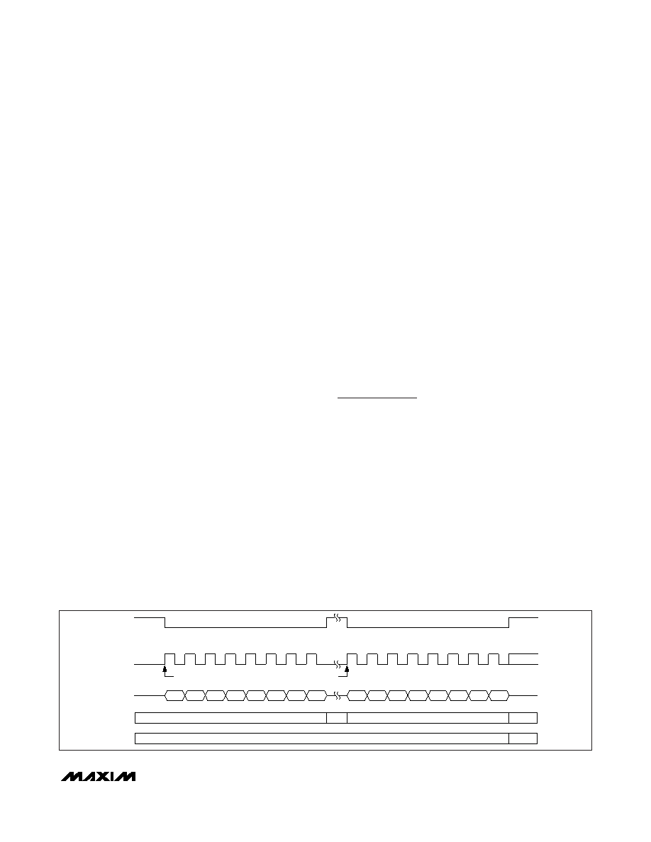
Figure 7. SPI Interface—Full Power-Down Mode
1ST SCLK RISING EDGE
0
D11
D10
D9
D8
D7
DOUT
MODE
SCLK
CNVST
0
000
0
FPD
RECOVERY
PPD
NORMAL
0
DOUT ENTERS TRI-STATE ONCE CNVST GOES HIGH
EXECUTE PARTIAL POWER-DOWN TWICE
FIRST 8-BIT TRANSFER
SECOND 8-BIT TRANSFER
REF
ENABLED (2.048V)
DISABLED
相关PDF资料 |
PDF描述 |
|---|---|
| MAX144ACUA+T | IC ADC 12BIT 108KSPS 8-UMAX |
| MAX144BEUA+T | IC ADC 12BIT 108KSPS 8-UMAX |
| MAX145ACUA+T | IC ADC 12BIT 108KSPS 8-UMAX |
| MAX145BEUA+T | IC ADC 12BIT 108KSPS 8-UMAX |
| MAX1166BCUP+T | IC ADC 16BIT PARALLEL 20-TSSOP |
相关代理商/技术参数 |
参数描述 |
|---|---|
| MAX1279BCTC | 功能描述:模数转换器 - ADC RoHS:否 制造商:Texas Instruments 通道数量:2 结构:Sigma-Delta 转换速率:125 SPs to 8 KSPs 分辨率:24 bit 输入类型:Differential 信噪比:107 dB 接口类型:SPI 工作电源电压:1.7 V to 3.6 V, 2.7 V to 5.25 V 最大工作温度:+ 85 C 安装风格:SMD/SMT 封装 / 箱体:VQFN-32 |
| MAX1279BCTC+ | 功能描述:模数转换器 - ADC Integrated Circuits (ICs) RoHS:否 制造商:Texas Instruments 通道数量:2 结构:Sigma-Delta 转换速率:125 SPs to 8 KSPs 分辨率:24 bit 输入类型:Differential 信噪比:107 dB 接口类型:SPI 工作电源电压:1.7 V to 3.6 V, 2.7 V to 5.25 V 最大工作温度:+ 85 C 安装风格:SMD/SMT 封装 / 箱体:VQFN-32 |
| MAX1279BCTC+T | 功能描述:模数转换器 - ADC Integrated Circuits (ICs) RoHS:否 制造商:Texas Instruments 通道数量:2 结构:Sigma-Delta 转换速率:125 SPs to 8 KSPs 分辨率:24 bit 输入类型:Differential 信噪比:107 dB 接口类型:SPI 工作电源电压:1.7 V to 3.6 V, 2.7 V to 5.25 V 最大工作温度:+ 85 C 安装风格:SMD/SMT 封装 / 箱体:VQFN-32 |
| MAX1279BCTC-T | 功能描述:模数转换器 - ADC RoHS:否 制造商:Texas Instruments 通道数量:2 结构:Sigma-Delta 转换速率:125 SPs to 8 KSPs 分辨率:24 bit 输入类型:Differential 信噪比:107 dB 接口类型:SPI 工作电源电压:1.7 V to 3.6 V, 2.7 V to 5.25 V 最大工作温度:+ 85 C 安装风格:SMD/SMT 封装 / 箱体:VQFN-32 |
| MAX1279BETC | 功能描述:模数转换器 - ADC RoHS:否 制造商:Texas Instruments 通道数量:2 结构:Sigma-Delta 转换速率:125 SPs to 8 KSPs 分辨率:24 bit 输入类型:Differential 信噪比:107 dB 接口类型:SPI 工作电源电压:1.7 V to 3.6 V, 2.7 V to 5.25 V 最大工作温度:+ 85 C 安装风格:SMD/SMT 封装 / 箱体:VQFN-32 |
发布紧急采购,3分钟左右您将得到回复。