- 您现在的位置:买卖IC网 > PDF目录9893 > MAX1292BEEG+T (Maxim Integrated Products)IC ADC 12BIT 400KSPS 24-QSOP PDF资料下载
参数资料
| 型号: | MAX1292BEEG+T |
| 厂商: | Maxim Integrated Products |
| 文件页数: | 2/20页 |
| 文件大小: | 0K |
| 描述: | IC ADC 12BIT 400KSPS 24-QSOP |
| 产品培训模块: | Lead (SnPb) Finish for COTS Obsolescence Mitigation Program |
| 标准包装: | 2,500 |
| 位数: | 12 |
| 采样率(每秒): | 400k |
| 数据接口: | 并联 |
| 转换器数目: | 1 |
| 功率耗散(最大): | 762mW |
| 电压电源: | 单电源 |
| 工作温度: | -40°C ~ 85°C |
| 安装类型: | 表面贴装 |
| 封装/外壳: | 24-SSOP(0.154",3.90mm 宽) |
| 供应商设备封装: | 24-QSOP |
| 包装: | 带卷 (TR) |
| 输入数目和类型: | 4 个单端,单极;4 个单端,双极;2 个伪差分,单极;2 个伪差分,双极 |
Analog Input Protection
Internal protection diodes, which clamp the analog
input to VDD and GND, allow each input channel to
swing within (GND - 300mV) to (VDD + 300mV) without
damage. However, for accurate conversions near full
scale, both inputs must not exceed (VDD + 50mV) or be
less than (GND - 50mV).
If an off-channel analog input voltage exceeds the sup-
plies by more than 50mV, limit the forward-bias input
current to 4mA.
Track/Hold
The MAX1290/MAX1292 T/H stage enters its tracking
mode on the rising edge of WR. In external acquisition
mode, the part enters its hold mode on the next rising
edge of WR. In internal acquisition mode, the part enters
its hold mode on the fourth falling edge of clock after
writing the control byte. Note that, in internal clock mode,
this is approximately 1s after writing the control byte.
In single-ended operation, IN- is connected to COM
and the converter samples the positive “+” input. In
pseudo-differential operation, IN- connects to the nega-
tive input “-” and the difference of |(IN+) - (IN-)| is sam-
pled. At the beginning of the next conversion, the
positive input connects back to IN+ and CHOLD
charges to the input signal.
The time required for the T/H stage to acquire an input
signal depends on how quickly its input capacitance is
charged. If the input signal’s source impedance is high,
the acquisition time lengthens and more time must be
allowed between conversions. The acquisition time,
tACQ, is the maximum time the device takes to acquire
the signal and is also the minimum time required for the
signal to be acquired. Calculate this with the following
equation:
tACQ = 9 (RS + RIN)CIN
where RS is the source impedance of the input signal,
RIN (800
) is the input resistance, and CIN (12pF) is
the input capacitance of the ADC. Source impedances
below 3k
have no significant impact on the MAX1290/
MAX1292’s AC performance.
Higher source impedances can be used if a 0.01F
capacitor is connected to the individual analog inputs.
Along with the input impedance, this capacitor forms
an RC filter, limiting the ADC’s signal bandwidth.
Input Bandwidth
The MAX1290/MAX1292 T/H stage offers a 350kHz full-
linear and a 6MHz full-power bandwidth that make it
possible to digitize high-speed transients and measure
periodic signals with bandwidths exceeding the ADC’s
sampling rate by using undersampling techniques. To
avoid aliasing high-frequency signals into the frequen-
cy band of interest, anti-alias filtering is recommended.
Starting a Conversion
Initiate a conversion by writing a control byte that
selects the multiplexer channel and configures the
MAX1290/MAX1292 for either unipolar or bipolar opera-
tion. A write pulse (WR + CS) can either start an acqui-
sition interval or initiate a combined acquisition plus
MAX1290/MAX1292
400ksps, +5V, 8-/4-Channel, 12-Bit ADCs
with +2.5V Reference and Parallel Interface
10
______________________________________________________________________________________
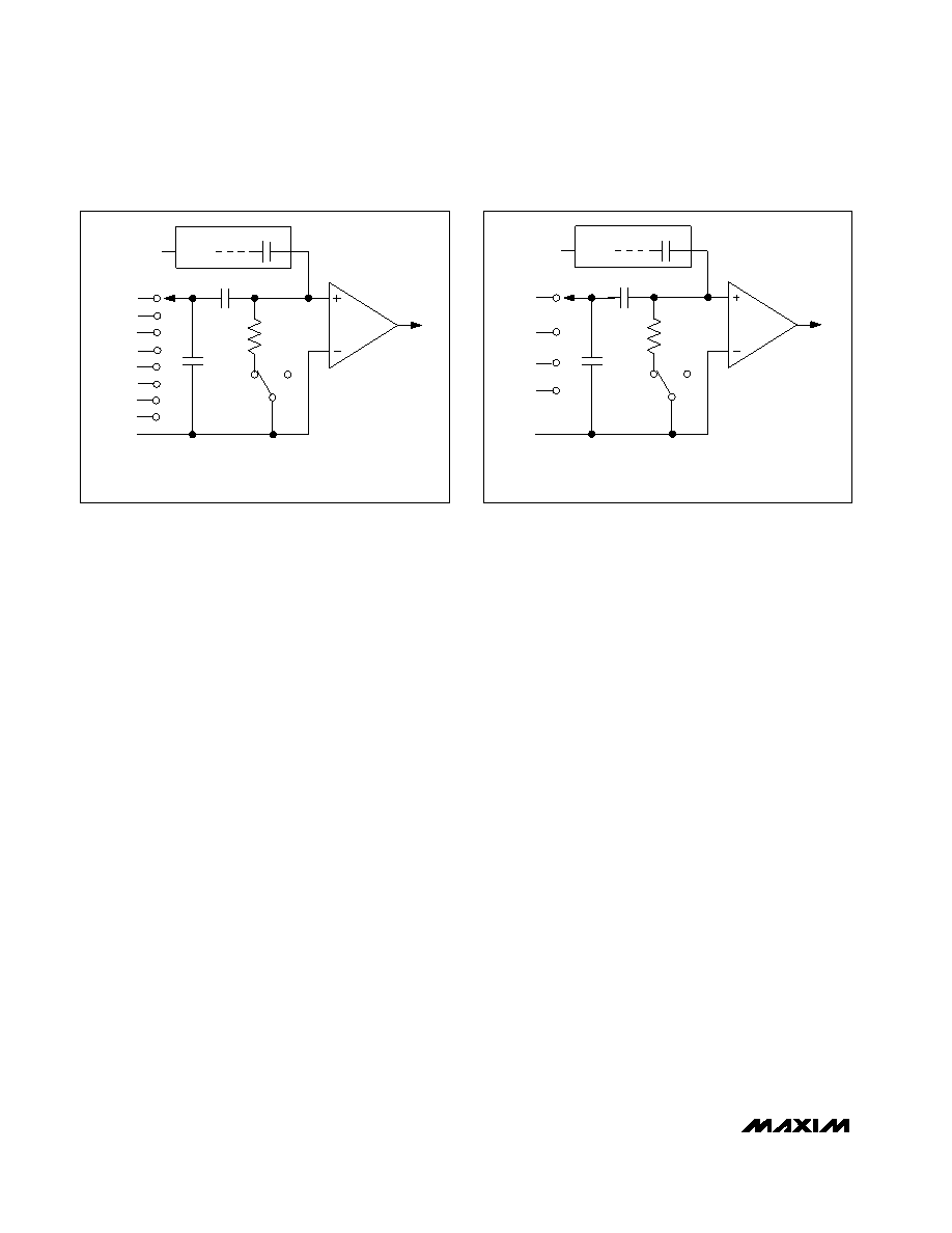
CH0
CH2
CH1
CH3
CH4
CH6
CH7
CH5
COM
CSWITCH
TRACK
T/H
SWITCH
RIN
800
CHOLD
HOLD
12-BIT CAPACITIVE DAC
REF
ZERO
COMPARATOR
–
+
12pF
SINGLE-ENDED MODE: IN+ = CH0–CH7, IN- = COM
PSEUDO-DIFFERENTIAL MODE: IN+ AND IN- SELECTED FROM PAIRS OF
CH0/CH1, CH2/CH3, CH4/CH5, AND CH6/CH7
AT THE SAMPLING INSTANT,
THE MUX INPUT SWITCHES
FROM THE SELECTED IN+
CHANNEL TO THE SELECTED
IN- CHANNEL.
INPUT
MUX
Figure 3a. MAX1290 Simplified Input Structure
CH0
CH1
CH2
CH3
COM
CSWITCH
TRACK
T/H
SWITCH
RIN
800
CHOLD
HOLD
12-BIT CAPACITIVE DAC
REF
ZERO
COMPARATOR
–
+
12pF
SINGLE-ENDED MODE: IN+ = CH0–CH3, IN- = COM
PSEUDO-DIFFERENTIAL MODE: IN+ AND IN- SELECTED FROM PAIRS OF
CH0/CH1 AND CH2/CH3
AT THE SAMPLING INSTANT,
THE MUX INPUT SWITCHES
FROM THE SELECTED IN+
CHANNEL TO THE SELECTED
IN- CHANNEL.
INPUT
MUX
Figure 3b. MAX1292 Simplified Input Structure
相关PDF资料 |
PDF描述 |
|---|---|
| IDT72V36110L7-5BBGI | IC FIFO 131KX36 7-5NS 144BGA |
| MAX1293ACEG+T | IC ADC 12BIT 250KSPS 24-QSOP |
| ISL32273EFVZ | IC RCVR RS485/422 QD ESD 16TSSOP |
| MAX184BCWG+T | IC ADC 12BIT HS 24-SOIC |
| ISL32179EFRZ | IC XMITTER ESD RS422 LP 24-QFN |
相关代理商/技术参数 |
参数描述 |
|---|---|
| MAX1292EVKIT | 功能描述:数据转换 IC 开发工具 MAX1292 Eval Kit RoHS:否 制造商:Texas Instruments 产品:Demonstration Kits 类型:ADC 工具用于评估:ADS130E08 接口类型:SPI 工作电源电压:- 6 V to + 6 V |
| MAX1293ACEG | 功能描述:模数转换器 - ADC Integrated Circuits (ICs) RoHS:否 制造商:Texas Instruments 通道数量:2 结构:Sigma-Delta 转换速率:125 SPs to 8 KSPs 分辨率:24 bit 输入类型:Differential 信噪比:107 dB 接口类型:SPI 工作电源电压:1.7 V to 3.6 V, 2.7 V to 5.25 V 最大工作温度:+ 85 C 安装风格:SMD/SMT 封装 / 箱体:VQFN-32 |
| MAX1293ACEG+ | 功能描述:模数转换器 - ADC 12-Bit 4Ch 250ksps 3.6V Precision ADC RoHS:否 制造商:Texas Instruments 通道数量:2 结构:Sigma-Delta 转换速率:125 SPs to 8 KSPs 分辨率:24 bit 输入类型:Differential 信噪比:107 dB 接口类型:SPI 工作电源电压:1.7 V to 3.6 V, 2.7 V to 5.25 V 最大工作温度:+ 85 C 安装风格:SMD/SMT 封装 / 箱体:VQFN-32 |
| MAX1293ACEG+T | 功能描述:模数转换器 - ADC 12-Bit 4Ch 250ksps 3.6V Precision ADC RoHS:否 制造商:Texas Instruments 通道数量:2 结构:Sigma-Delta 转换速率:125 SPs to 8 KSPs 分辨率:24 bit 输入类型:Differential 信噪比:107 dB 接口类型:SPI 工作电源电压:1.7 V to 3.6 V, 2.7 V to 5.25 V 最大工作温度:+ 85 C 安装风格:SMD/SMT 封装 / 箱体:VQFN-32 |
| MAX1293ACEG-T | 功能描述:模数转换器 - ADC RoHS:否 制造商:Texas Instruments 通道数量:2 结构:Sigma-Delta 转换速率:125 SPs to 8 KSPs 分辨率:24 bit 输入类型:Differential 信噪比:107 dB 接口类型:SPI 工作电源电压:1.7 V to 3.6 V, 2.7 V to 5.25 V 最大工作温度:+ 85 C 安装风格:SMD/SMT 封装 / 箱体:VQFN-32 |
发布紧急采购,3分钟左右您将得到回复。