- 您现在的位置:买卖IC网 > PDF目录9891 > MAX1294BEEI+T (Maxim Integrated Products)IC ADC 12BIT 420KSPS 28-QSOP PDF资料下载
参数资料
| 型号: | MAX1294BEEI+T |
| 厂商: | Maxim Integrated Products |
| 文件页数: | 17/19页 |
| 文件大小: | 0K |
| 描述: | IC ADC 12BIT 420KSPS 28-QSOP |
| 产品培训模块: | Lead (SnPb) Finish for COTS Obsolescence Mitigation Program |
| 标准包装: | 2,500 |
| 位数: | 12 |
| 采样率(每秒): | 420k |
| 数据接口: | 并联 |
| 转换器数目: | 1 |
| 功率耗散(最大): | 667mW |
| 电压电源: | 单电源 |
| 工作温度: | -40°C ~ 85°C |
| 安装类型: | 表面贴装 |
| 封装/外壳: | 28-SSOP(0.154",3.90mm 宽) |
| 供应商设备封装: | 28-QSOP |
| 包装: | 带卷 (TR) |
| 输入数目和类型: | 6 个单端,单极;6 个单端,双极;3 个伪差分,单极;3 个伪差分,双极 |
MAX1294/MAX1296
420ksps, +5V, 6-/2-Channel, 12-Bit ADCs
with +2.5V Reference and Parallel Interface
_______________________________________________________________________________________
7
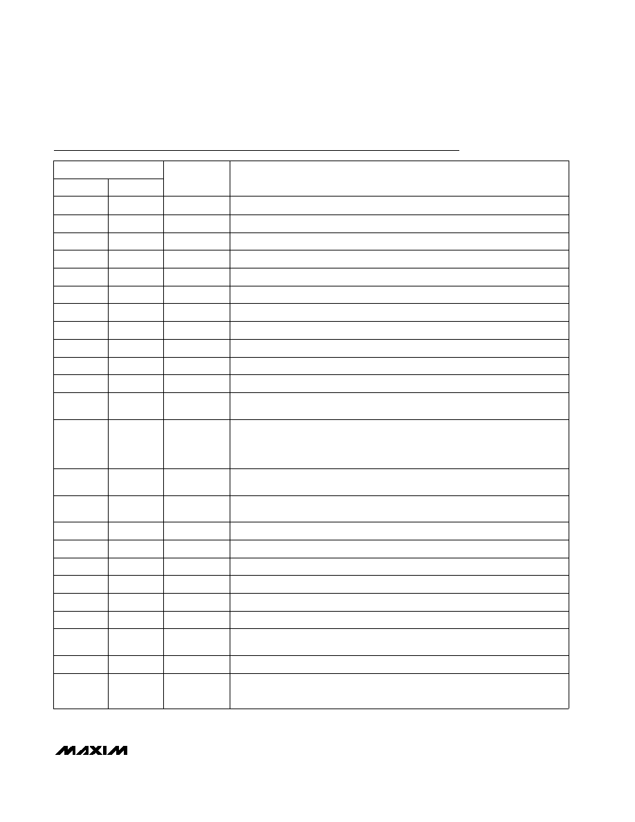
Pin Description
D0
10
INT
11
RD
12
WR
13
CLK
14
D4
6
D3
7
D2
8
D1
9
D5
5
D6
4
1
D7
3
D8
2
D9
1
Three-State Digital I/O Line (D0)
INT goes low when the conversion is complete and output data is ready.
Active-Low Read Select. If CS is low, a falling edge on RD enables the read
operation on the data bus.
Active-Low Write Select. When CS is low in the internal acquisition mode, a rising
edge on WR latches in configuration data and starts an acquisition plus a conver-
sion cycle. When CS is low in external acquisition mode, the first rising edge on WR
ends acquisition and starts a conversion.
Clock Input. In external clock mode, drive CLK with a TTL/CMOS-compatible clock.
In internal clock mode, connect this pin to either VDD or GND.
Three-State Digital I/O Line (D4)
Three-State Digital I/O Line (D3)
Three-State Digital I/O Line (D2)
Three-State Digital I/O Line (D1)
Three-State Digital I/O Line (D5)
Three-State Digital I/O Line (D6)
Three-State Digital I/O Line (D7)
Three-State Digital Output (D8)
Three-State Digital Output (D9)
GND
19
23
REFADJ
20
24
CH2
—
19
CH1
16
20
CH0
17
21
COM
18
22
CH3
—
18
CH4
—
17
CH5
—
16
CS
15
Analog and Digital Ground
Bandgap Reference Output/Bandgap Reference Buffer Input. Bypass to GND with
a 0.01F capacitor. When using an external reference, connect REFADJ to VDD to
disable the internal bandgap reference.
Analog Input Channel 2
Analog Input Channel 1
Analog Input Channel 0
Ground Reference for Analog Inputs. Sets zero-code voltage in single-ended mode
and must be stable to ±0.5 LSB during conversion.
Analog Input Channel 3
Analog Input Channel 4
Analog Input Channel 5
Active-Low Chip Select. When CS is high, digital outputs (INT, D11–D0) are high
impedance.
PIN
MAX1296
MAX1294
NAME
FUNCTION
相关PDF资料 |
PDF描述 |
|---|---|
| IDT72T7295L6-7BB | IC FIFO 32768X72 6-7NS 324-BGA |
| MS27468E21A1P | CONN RCPT 79POS JAM NUT W/PINS |
| MAX1295BEEI+T | IC ADC 12BIT 265KSPS 28-QSOP |
| MS27484E16A26S | CONN PLUG 26POS STRAIGHT W/SCKT |
| MAX1295ACEI+T | IC ADC 12BIT 265KSPS 28-QSOP |
相关代理商/技术参数 |
参数描述 |
|---|---|
| MAX1294EVKIT | 功能描述:数据转换 IC 开发工具 MAX1294 Eval Kit RoHS:否 制造商:Texas Instruments 产品:Demonstration Kits 类型:ADC 工具用于评估:ADS130E08 接口类型:SPI 工作电源电压:- 6 V to + 6 V |
| MAX1295ACEI | 功能描述:模数转换器 - ADC RoHS:否 制造商:Texas Instruments 通道数量:2 结构:Sigma-Delta 转换速率:125 SPs to 8 KSPs 分辨率:24 bit 输入类型:Differential 信噪比:107 dB 接口类型:SPI 工作电源电压:1.7 V to 3.6 V, 2.7 V to 5.25 V 最大工作温度:+ 85 C 安装风格:SMD/SMT 封装 / 箱体:VQFN-32 |
| MAX1295ACEI+ | 功能描述:模数转换器 - ADC 12-Bit 6Ch 265ksps 3.6V Precision ADC RoHS:否 制造商:Texas Instruments 通道数量:2 结构:Sigma-Delta 转换速率:125 SPs to 8 KSPs 分辨率:24 bit 输入类型:Differential 信噪比:107 dB 接口类型:SPI 工作电源电压:1.7 V to 3.6 V, 2.7 V to 5.25 V 最大工作温度:+ 85 C 安装风格:SMD/SMT 封装 / 箱体:VQFN-32 |
| MAX1295ACEI+T | 功能描述:模数转换器 - ADC 12-Bit 6Ch 265ksps 3.6V Precision ADC RoHS:否 制造商:Texas Instruments 通道数量:2 结构:Sigma-Delta 转换速率:125 SPs to 8 KSPs 分辨率:24 bit 输入类型:Differential 信噪比:107 dB 接口类型:SPI 工作电源电压:1.7 V to 3.6 V, 2.7 V to 5.25 V 最大工作温度:+ 85 C 安装风格:SMD/SMT 封装 / 箱体:VQFN-32 |
| MAX1295ACEI-T | 功能描述:模数转换器 - ADC RoHS:否 制造商:Texas Instruments 通道数量:2 结构:Sigma-Delta 转换速率:125 SPs to 8 KSPs 分辨率:24 bit 输入类型:Differential 信噪比:107 dB 接口类型:SPI 工作电源电压:1.7 V to 3.6 V, 2.7 V to 5.25 V 最大工作温度:+ 85 C 安装风格:SMD/SMT 封装 / 箱体:VQFN-32 |
发布紧急采购,3分钟左右您将得到回复。