- 您现在的位置:买卖IC网 > PDF目录8943 > MAX13055EEWG+T (Maxim Integrated Products)IC TRANSLATOR LL 8CH 24WLP PDF资料下载
参数资料
| 型号: | MAX13055EEWG+T |
| 厂商: | Maxim Integrated Products |
| 文件页数: | 7/14页 |
| 文件大小: | 0K |
| 描述: | IC TRANSLATOR LL 8CH 24WLP |
| 产品培训模块: | Lead (SnPb) Finish for COTS Obsolescence Mitigation Program |
| 标准包装: | 1 |
| 逻辑功能: | 变换器,双向,开路漏极 |
| 位数: | 8 |
| 输入类型: | 电压 |
| 输出类型: | 电压 |
| 通道数: | 8 |
| 输出/通道数目: | 1 |
| 差分 - 输入:输出: | 无/无 |
| 工作温度: | -40°C ~ 85°C |
| 封装/外壳: | 24-WFBGA,WLCSP |
| 供应商设备封装: | 24-WLP |
| 包装: | 标准包装 |
| 其它名称: | MAX13055EEWG+TDKR |
MAX13055E–MAX13058E
1.62V to 3.6V, 8-Channel, High-Speed LLT
2
_______________________________________________________________________________________
ABSOLUTE MAXIMUM RATINGS
Stresses beyond those listed under “Absolute Maximum Ratings” may cause permanent damage to the device. These are stress ratings only, and functional
operation of the device at these or any other conditions beyond those indicated in the operational sections of the specifications is not implied. Exposure to
absolute maximum rating conditions for extended periods may affect device reliability.
(Voltages referenced to GND.)
VCC, VL .............................................................................-0.3V to +4.0V
EN..........................................................................-0.3V to +4.0V
I/O VCC_ .....................................................-0.3V to (VCC + 0.3V)
I/O VL_ ...........................................................-0.3V to (VL + 0.3V)
Short-Circuit Duration
I/O to GND..................................................................Continuous
Continuous Power Dissipation (TA = +70°C)
28-Pin TQFN (derate 28.6mW/°C above +70°C) .......2286mW
Junction-to-Case Thermal Resistance (
θJC) (Note 1)
28-Pin TQFN................................................................2.7°C/W
Junction-to-Ambient Thermal Resistance (
θJA) (Note 1)
24-Bump WLP ..............................................................97°C/W
28-Pin TQFN.................................................................35°C/W
Operating Temperature Range ...........................-40°C to +85°C
Junction Temperature ......................................................+150°C
Storage Temperature Range .............................-65°C to +150°C
Lead Temperature (soldering, 10s) .................................+300°C
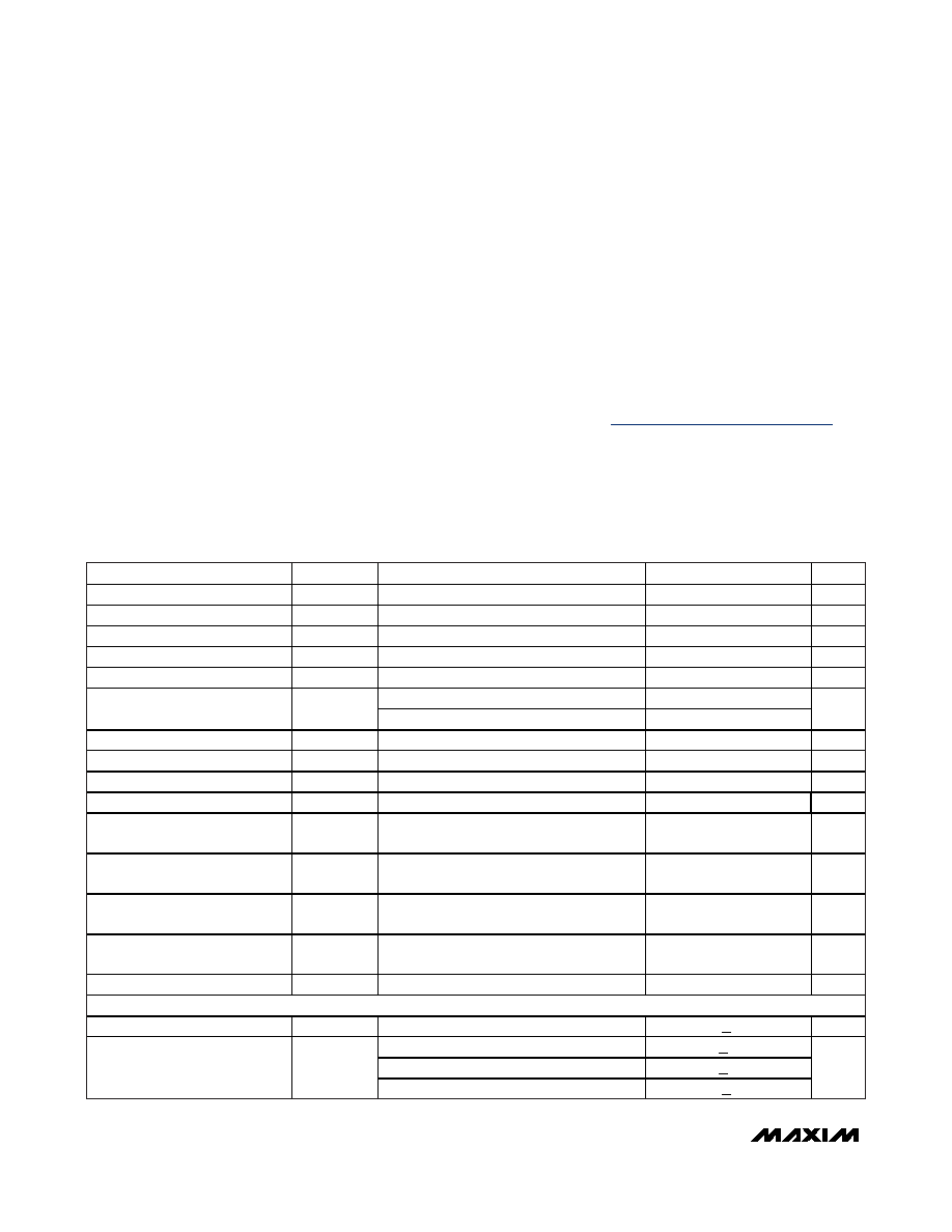
ELECTRICAL CHARACTERISTICS
(VCC = +2.2V to +3.6V, VL = +1.62V to +3.2V, EN = VL, TA = -40°C to +85°C, unless otherwise noted. Typical values are at VCC = +3.3V,
VL = +1.8V, and TA = +25°C.) (Notes 2, 3)
PARAMETER
SYMBOL
CONDITIONS
MIN
TYP
MAX
UNITS
VL Supply Range
VL
1.62
3.2
V
VCC Supply Range
VCC
2.2
3.6
V
Supply Current from VCC
IQVCC
I/O VCC_ = VCC, I/O VL_ = VL
40
A
Supply Current from VL
IQVL
I/O VCC_ = VCC, I/O VL_ = VL
10
A
VCC Shutdown Supply Current
ISHDN-VCC
TA = +25°C, EN = GND
0.1
2
A
TA = +25°C, EN = GND
0.1
1
VL Shutdown Mode Supply
Current
ISHDN-VL
TA = +25°C, EN = VL, VCC = 0V
0.1
4
A
I/O Three-State Leakage Current
ILEAK
TA = +25°C, EN = GND
0.1
2
A
EN Input Leakage Current
ILEAK_EN
TA = +25
oC1
A
VL - VCC Shutdown Threshold HighVTH_H
VCC rising
0
0.1 x VL
0.8
V
VL - VCC Shutdown Threshold Low
VTH_L
VCC falling
0
0.12 x VL
0.8
V
I/O VCC_ Pulldown Resistance
During Shutdown
RVCC_PD_SD MAX13056E/MAX13058E
10
16.5
23
k
Ω
I/O VL_ Pulldown Resistance
During Shutdown
RVL_PD_SD
MAX13057E/MAX13058E
10
16.5
23
k
Ω
I/O VL_ Pullup Current
(Normal Mode)
IVL_PU_
I/O VL_ = GND, I/O VCC_ = GND
20
65
A
I/O VCC_ Pullup Current
(Normal Mode)
IVCC_PU_
I/O VCC_ = GND, I/O VL_ = GND
20
65
A
I/O VL_ to I/O VCC_ DC Resistance
RIOVL_IOVCC
3k
Ω
ESD PROTECTION
All Ports
Human Body Model
+2kV
Human Body Model
+15
IEC 61000-4-2 Air-Gap Discharge, CVCC = 1F
+15
I/O VCC_ Only
IEC 61000-4-2 Contact Discharge, CVCC = 1F
+8
kV
Note 1: Package thermal resistances were obtained using the method described in JEDEC specification JESD51-7, using a four-
layer board. For detailed information on package thermal considerations, refer to www.maxim-ic.com/thermal-tutorial.
相关PDF资料 |
PDF描述 |
|---|---|
| MAX13030EEBE+T | IC TRANSLATOR LL 6CH 16UCSP |
| VI-J1Y-MZ-F1 | CONVERTER MOD DC/DC 3.3V 16.5W |
| VE-B0F-MY-F3 | CONVERTER MOD DC/DC 72V 50W |
| VI-J0J-MZ-F2 | CONVERTER MOD DC/DC 36V 25W |
| MAX13003EEUE+ | IC LEVEL TRANS 6CH 16-TSSOP |
相关代理商/技术参数 |
参数描述 |
|---|---|
| MAX13058EETI+ | 功能描述:转换 - 电压电平 1.62V to 3.6V 8-Channel High-Speed LLT RoHS:否 制造商:Micrel 类型:CML/LVDS/LVPECL to LVCMOS/LVTTL 传播延迟时间:1.9 ns 电源电流:14 mA 电源电压-最大:3.6 V 电源电压-最小:3 V 最大工作温度:+ 85 C 安装风格:SMD/SMT 封装 / 箱体:MLF-8 |
| MAX13058EETI+T | 功能描述:转换 - 电压电平 1.62V to 3.6V 8-Channel High-Speed LLT RoHS:否 制造商:Micrel 类型:CML/LVDS/LVPECL to LVCMOS/LVTTL 传播延迟时间:1.9 ns 电源电流:14 mA 电源电压-最大:3.6 V 电源电压-最小:3 V 最大工作温度:+ 85 C 安装风格:SMD/SMT 封装 / 箱体:MLF-8 |
| MAX13058EEWG+ | 制造商:Rochester Electronics LLC 功能描述: 制造商:Maxim Integrated Products 功能描述: |
| MAX13058EEWG+T | 功能描述:转换 - 电压电平 100Mbps, 8-Ch, Bidir Ectional Level Trans RoHS:否 制造商:Micrel 类型:CML/LVDS/LVPECL to LVCMOS/LVTTL 传播延迟时间:1.9 ns 电源电流:14 mA 电源电压-最大:3.6 V 电源电压-最小:3 V 最大工作温度:+ 85 C 安装风格:SMD/SMT 封装 / 箱体:MLF-8 |
| MAX1305ECM | 功能描述:模数转换器 - ADC RoHS:否 制造商:Texas Instruments 通道数量:2 结构:Sigma-Delta 转换速率:125 SPs to 8 KSPs 分辨率:24 bit 输入类型:Differential 信噪比:107 dB 接口类型:SPI 工作电源电压:1.7 V to 3.6 V, 2.7 V to 5.25 V 最大工作温度:+ 85 C 安装风格:SMD/SMT 封装 / 箱体:VQFN-32 |
发布紧急采购,3分钟左右您将得到回复。