- 您现在的位置:买卖IC网 > PDF目录2086 > MAX13101EETL+T (Maxim Integrated Products)IC TRANSLATOR LL 16CH 40TQFN PDF资料下载
参数资料
| 型号: | MAX13101EETL+T |
| 厂商: | Maxim Integrated Products |
| 文件页数: | 1/18页 |
| 文件大小: | 0K |
| 描述: | IC TRANSLATOR LL 16CH 40TQFN |
| 产品培训模块: | Lead (SnPb) Finish for COTS Obsolescence Mitigation Program |
| 标准包装: | 1 |
| 逻辑功能: | 变换器,双向,3 态 |
| 位数: | 16 |
| 输入类型: | CMOS |
| 输出类型: | CMOS |
| 数据速率: | 20Mbps |
| 通道数: | 16 |
| 输出/通道数目: | 1 |
| 差分 - 输入:输出: | 无/无 |
| 传输延迟(最大): | 20ns |
| 电源电压: | 1.65 V ~ 5.5 V |
| 工作温度: | -40°C ~ 85°C |
| 封装/外壳: | 40-WFQFN 裸露焊盘 |
| 供应商设备封装: | 40-TQFN-EP(5x5) |
| 包装: | 标准包装 |
| 其它名称: | MAX13101EETL+TDKR |
MAX13101E/MAX13102E/
MAX13103E/MAX13108E
16-Channel Buffered CMOS
Logic-Level Translators
19-3802; Rev 4; 7/13
For pricing, delivery, and ordering information, please contact Maxim Direct
at 1-888-629-4642, or visit Maxim’s website at www.maximintegrated.com.
General Description
The MAX13101E/MAX13102E/MAX13103E/MAX13108E
16-bit bidirectional CMOS logic-level translators pro-
vide the level shifting necessary to allow data transfer in
multivoltage systems. These devices are inherently
bidirectional due to their design and do not require the
use of a direction input. Externally applied voltages,
VCC and VL, set the logic levels on either side of the
devices. Logic signals present on the VL side of the
device appear as a higher voltage logic signal on the
VCC side of the device, and vice-versa.
The MAX13101E/MAX13102E/MAX13103E feature an
enable input (EN) that, when low, reduces the VCC and
VL supply currents to less than 2A. The MAX13108E
features a multiplexing input (MULT) that selects one
byte between the two, thus allowing multiplexing of the
signals. The MAX13101E/MAX13102E/MAX13103E/
MAX13108E have ±15kV ESD protection on the I/O VCC
side for greater protection in applications that route sig-
nals externally. Three different output configurations are
available during shutdown, allowing the I/O on the VCC
side or the VL side to be put in a high-impedance state
or pulled to ground through an internal 6k
Ω resistor.
The MAX13101E/MAX13102E/MAX13103E/MAX13108E
accept VCC voltages from +1.65V to +5.5V and VL
voltages from +1.2V to VCC, making them ideal for data
transfer between low-voltage ASICs/PLDs and higher
voltage systems. The MAX13101E/MAX13102E/
MAX13103E/MAX13108E are available in 36-bump
WLP and 40-pin TQFN packages, and operate over the
extended -40°C to +85°C temperature range. See the
Ordering Information.
Applications
Features
o Wide Supply Voltage Range
VCC Range of 1.65V to 5.5V
VL Range of 1.2V to VCC
o ESD Protection on I/O VCC Lines
±15kV Human Body Model
o Up to 20Mbps Throughput
o Low 0.03A Typical Quiescent Current
o WLP and TQFN Packages
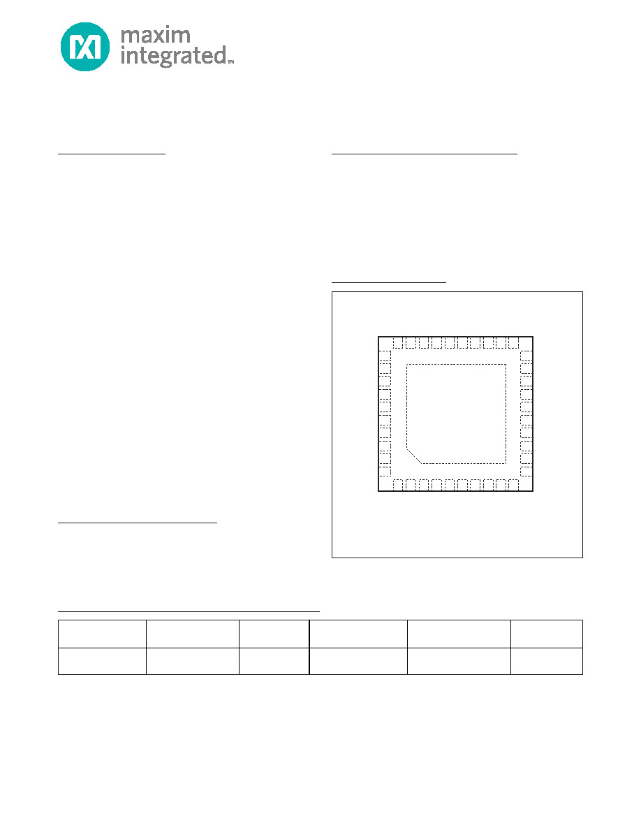
Pin Configurations
Ordering Information/Selector Guide continued at end of data sheet.
Ordering Information/Selector Guide
PART
PIN-PACKAGE
DATA
RATE (Mbps)
I/O VL STATE
DURING SHUTDOWN
I/O VCC STATE
DURING SHUTDOWN
MULTIPLEXER
FEATURE
MAX13101EETL+
40 TQFN-EP*
5mm x 5mm x 0.8mm
20
High impedance
6k
Ω to GND
No
Note: All devices are specified over the -40°C to +85°C operating temperature range.
MAX13101E
MAX13102E
MAX13103E
TQFN
+
TOP VIEW OF BOTTOM LEADS
56
4
3
I/O VL14
I/O VL16
VL
VCC
I/O VCC16
I/O VL13
I/O VL3
I/O VL1
VL
I/O VL4
VCC
I/O VCC1
11
12
I/O
V
L7
14
15
16
17
I/O
V
L8
I/O
V
L9
I/O
V
CC
7
I/O
V
CC
8
I/O
V
CC
9
I/O
V
CC
10
I/O VL15
I/O VL2
13
7
I/O
V
L10
I/O
V
CC
11
8
*EXPOSED PAD CONNECTED TO GROUND
I/O
V
L11
I/O
V
L12
EN
I/O
V
CC
12
GND
9
10
I/O
V
L6
2
I/O
V
CC
6
I/O
V
L5
1
I/O
V
CC
5
GND
26
25
27
28
24
23
22
21
29
30
I/O VCC15
I/O VCC14
I/O VCC13
I/O VCC2
I/O VCC3
I/O VCC4
18
19
20
40
39
37
36
35
34
38
33
32
31
GND
*EP
CMOS Logic-Level
Translation
Portable Equipment
Cell Phones
PDAs
Digital Still Cameras
Smart Phones
+
Denotes a lead-free/RoHS-compliant package.
*
EP = Exposed pad.
Pin Configurations continued at end of data sheet.
Typical Operating Circuit appears at end of data sheet.
相关PDF资料 |
PDF描述 |
|---|---|
| MAX13326GUI/V+T | IC AUD LINE DVR DL AUTO 28TSSOP |
| MAX13331GEE/V+T | IC AMP STEREO HEADPHONE 16-QSOP |
| MAX133EPL+ | IC DMM CIRC 3 3/4 DIG 40-DIP |
| MAX1379ATP+ | IC ADC 12BIT 1.25MSPS DL 20-TQFN |
| MAX138EPL+ | IC ADC 3 1/2DIG W/LCD DVR 40-DIP |
相关代理商/技术参数 |
参数描述 |
|---|---|
| MAX13102EEBX | 制造商:Rochester Electronics LLC 功能描述: 制造商:Maxim Integrated Products 功能描述: |
| MAX13102EEBX-T | 制造商:Rochester Electronics LLC 功能描述: 制造商:Maxim Integrated Products 功能描述: |
| MAX13102EETL+ | 功能描述:转换 - 电压电平 16-Ch 20Mbps 5.5V Logic Level Tr RoHS:否 制造商:Micrel 类型:CML/LVDS/LVPECL to LVCMOS/LVTTL 传播延迟时间:1.9 ns 电源电流:14 mA 电源电压-最大:3.6 V 电源电压-最小:3 V 最大工作温度:+ 85 C 安装风格:SMD/SMT 封装 / 箱体:MLF-8 |
| MAX13102EETL+T | 功能描述:转换 - 电压电平 16-Ch 20Mbps 5.5V Logic Level Tr RoHS:否 制造商:Micrel 类型:CML/LVDS/LVPECL to LVCMOS/LVTTL 传播延迟时间:1.9 ns 电源电流:14 mA 电源电压-最大:3.6 V 电源电压-最小:3 V 最大工作温度:+ 85 C 安装风格:SMD/SMT 封装 / 箱体:MLF-8 |
| MAX13103EEBX | 制造商:Rochester Electronics LLC 功能描述: 制造商:Maxim Integrated Products 功能描述: |
发布紧急采购,3分钟左右您将得到回复。