- 您现在的位置:买卖IC网 > PDF目录8843 > MAX13102EETL+T (Maxim Integrated Products)IC XLATOR 16CH BUFF LL 40-TQFN PDF资料下载
参数资料
| 型号: | MAX13102EETL+T |
| 厂商: | Maxim Integrated Products |
| 文件页数: | 5/18页 |
| 文件大小: | 0K |
| 描述: | IC XLATOR 16CH BUFF LL 40-TQFN |
| 产品培训模块: | Lead (SnPb) Finish for COTS Obsolescence Mitigation Program |
| 标准包装: | 2,500 |
| 逻辑功能: | 变换器,双向,3 态 |
| 位数: | 16 |
| 输入类型: | CMOS |
| 输出类型: | CMOS |
| 数据速率: | 20Mbps |
| 通道数: | 16 |
| 输出/通道数目: | 1 |
| 差分 - 输入:输出: | 无/无 |
| 传输延迟(最大): | 20ns |
| 电源电压: | 1.65 V ~ 5.5 V |
| 工作温度: | -40°C ~ 85°C |
| 封装/外壳: | 40-WFQFN 裸露焊盘 |
| 供应商设备封装: | 40-TQFN-EP(5x5) |
| 包装: | 带卷 (TR) |
MAX13101E/MAX13102E/
MAX13103E/MAX13108E
16-Channel Buffered CMOS
Logic-Level Translators
13
Maxim Integrated
Detailed Description
The MAX13101E/MAX13102E/MAX13103E/MAX13108E
logic-level translators provide the level shifting neces-
sary to allow data transfer in a multivoltage system.
Externally applied voltages, VCC and VL, set the logic
levels on either side of the device. Logic signals pre-
sent on the VL side of the device appear as a higher
voltage logic signal on the VCC side of the device, and
vice-versa. The MAX13101E/MAX13102E/MAX13103E/
MAX13108E are bidirectional level translators allowing
data translation in either direction (VL
VCC) on
any single data line. The MAX13101E/MAX13102E/
MAX13103E/MAX13108E accept VL from +1.2V to VCC.
All devices have a VCC range from +1.65V to +5.5V,
making them ideal for data transfer between low-volt-
age ASICs/PLDs and higher voltage systems.
The MAX13101E/MAX13102E/MAX13103E feature an
output enable mode that reduces VCC supply current to
less than 1A, and VL supply current to less than 2A
when in shutdown. The MAX13108E features a multi-
plexing input that selects one byte between the two,
thus allowing multiplexing of the signals. The
MAX13101E/MAX13102E/MAX13103E/MAX13108E
have ±15kV ESD protection on the I/O VCC side for
greater protection in applications that route signals
externally. The MAX13101E/MAX13102E/MAX13103E/
MAX13108E operate at a guaranteed data rate of
20Mbps. The maximum data rate depends heavily
on the load capacitance (see the
Typical Operating
Characteristics) and the output impedance of the
external driver.
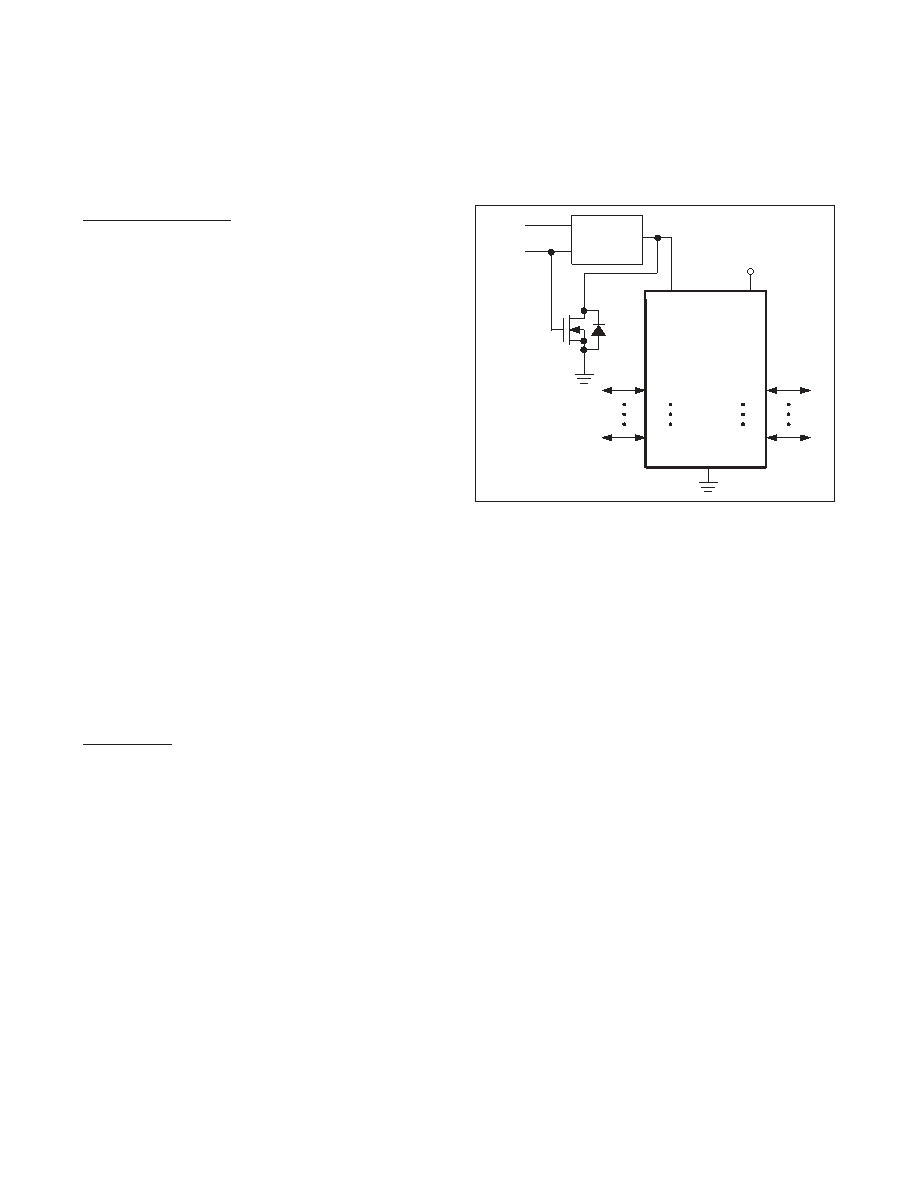
Power-Supply Sequencing
For proper operation, ensure that +1.65V
≤ VCC ≤ +5.5V,
+1.2V
≤ VL ≤ +5.5V, and VL ≤ VCC. During power-up
sequencing, VL ≥ VCC does not damage the device.
When VCC is disconnected and VL is powering up, up to
10mA of current can be sourced to each load on the VL
side, yet the device does not latch up. To guarantee that
no excess leakage current flows and that the device
does not interfere with the I/O on the VL side, VCC should
be connected to GND with a max 50
Ω resistor when the
VCC supply is not present (Figure 5).
Input Driver Requirements
The MAX13101E/MAX13102E/MAX13103E/MAX13108E
architecture is based on a one-shot accelerator output
stage (Figure 6). Accelerator output stages are always
in tri-state except when there is a transition on any of
the translators on the input side, either I/O VL_ or
I/O VCC_. Then a short pulse is generated, during
which the accelerator output stages become active and
charge/discharge the capacitances at the I/Os. Due to
the bidirectional nature, both input stages become
active during the one-shot pulse. This can lead to some
current feeding into the external source that is driving
the translator. However, this behavior helps to speed
up the transition on the driven side.
For proper full-speed operation, the output current of a
device that drives the inputs of the MAX13101E/
MAX13102E/MAX13103E/MAX13108E should meet the
following requirement:
i > 108 x V x (C + 10pF)
where, i is the driver output current, V is the logic-supply
voltage (i.e., VL or VCC) and C is the parasitic capaci-
tance of the signal line.
Enable Output Mode (EN)
The MAX13101E/MAX13102E/MAX13103E feature an
enable input (EN) that, when driven low, places the
device into shutdown mode. During shutdown, the
MAX13101E I/O VCC_ ports are pulled down to ground
with internal 6k
Ω resistors and the I/O VL _ ports enter
tri-state. MAX13102E I/O VCC_ lines enter tri-state and
the I/OVL _ lines are pulled down to ground with internal
6k
Ω resistors. All I/O VCC_ and I/O VL _ lines on the
MAX13103E enter tri-state while the device is in shut-
down mode. During shutdown, the VCC supply current
reduces to less than 1A, and the VL supply current
reduces to less than 2A. To guarantee minimum shut-
down supply current, all I/O VL _ need to be driven to
GND or VL, or pulled to GND or VL through 100kΩ
resistors. All I/O VCC_ need to be driven to GND or
VCC, or pulled to GND or VCC through 100kΩ resistors.
Drive EN to logic-high (VL or VCC) for normal operation.
I/O VCC16
I/O VL16
I/O VL1
I/O VCC1
VCC
VL
+1.2V TO +5.5V
GND
VCC SUPPLY
VBATT
DISABLE
RDSON < 50
Ω
MAX13101E
MAX13102E
MAX13103E
MAX13108E
Figure 5. Recommended Circuit for Powering Down VCC
相关PDF资料 |
PDF描述 |
|---|---|
| VI-261-MY-F3 | CONVERTER MOD DC/DC 12V 50W |
| MS27505E21F41PLC | CONN HSG RCPT 41POS BOX MNT PINS |
| V150B5M200BF3 | CONVERTER MOD DC/DC 5V 200W |
| MAX13101EETL+ | IC TRANSL LOGIC 16CH 40-TQFN |
| V150B5M200BF2 | CONVERTER MOD DC/DC 5V 200W |
相关代理商/技术参数 |
参数描述 |
|---|---|
| MAX13103EEBX | 制造商:Rochester Electronics LLC 功能描述: 制造商:Maxim Integrated Products 功能描述: |
| MAX13103EEBX-T | 制造商:Rochester Electronics LLC 功能描述: 制造商:Maxim Integrated Products 功能描述: |
| MAX13103EETL | 功能描述:转换 - 电压电平 RoHS:否 制造商:Micrel 类型:CML/LVDS/LVPECL to LVCMOS/LVTTL 传播延迟时间:1.9 ns 电源电流:14 mA 电源电压-最大:3.6 V 电源电压-最小:3 V 最大工作温度:+ 85 C 安装风格:SMD/SMT 封装 / 箱体:MLF-8 |
| MAX13103EETL+ | 功能描述:转换 - 电压电平 16-Ch 20Mbps 5.5V Logic Level Tr RoHS:否 制造商:Micrel 类型:CML/LVDS/LVPECL to LVCMOS/LVTTL 传播延迟时间:1.9 ns 电源电流:14 mA 电源电压-最大:3.6 V 电源电压-最小:3 V 最大工作温度:+ 85 C 安装风格:SMD/SMT 封装 / 箱体:MLF-8 |
| MAX13103EETL+T | 功能描述:转换 - 电压电平 16-Ch 20Mbps 5.5V Logic Level Tr RoHS:否 制造商:Micrel 类型:CML/LVDS/LVPECL to LVCMOS/LVTTL 传播延迟时间:1.9 ns 电源电流:14 mA 电源电压-最大:3.6 V 电源电压-最小:3 V 最大工作温度:+ 85 C 安装风格:SMD/SMT 封装 / 箱体:MLF-8 |
发布紧急采购,3分钟左右您将得到回复。