- 您现在的位置:买卖IC网 > PDF目录10552 > MAX1320ECM+ (Maxim Integrated Products)IC ADC 14BIT 8CH 2MSPS 48LQFP PDF资料下载
参数资料
| 型号: | MAX1320ECM+ |
| 厂商: | Maxim Integrated Products |
| 文件页数: | 6/27页 |
| 文件大小: | 0K |
| 描述: | IC ADC 14BIT 8CH 2MSPS 48LQFP |
| 产品培训模块: | Lead (SnPb) Finish for COTS Obsolescence Mitigation Program |
| 标准包装: | 250 |
| 位数: | 14 |
| 采样率(每秒): | 2M |
| 数据接口: | 并联 |
| 转换器数目: | 1 |
| 功率耗散(最大): | 1.82W |
| 电压电源: | 模拟和数字 |
| 工作温度: | -40°C ~ 85°C |
| 安装类型: | 表面贴装 |
| 封装/外壳: | 48-LQFP |
| 供应商设备封装: | 48-LQFP(7x7) |
| 包装: | 管件 |
| 输入数目和类型: | 8 个单端,双极 |
第1页第2页第3页第4页第5页当前第6页第7页第8页第9页第10页第11页第12页第13页第14页第15页第16页第17页第18页第19页第20页第21页第22页第23页第24页第25页第26页第27页
MAX1316–MAX1318/MAX1320–MAX1322/MAX1324–MAX1326
8-/4-/2-Channel, 14-Bit, Simultaneous-Sampling ADCs
with ±10V, ±5V, and 0 to +5V Analog Input Ranges
14
______________________________________________________________________________________
To improve the input-signal bandwidth under AC condi-
tions, drive the input with a wideband buffer (>50MHz)
that can drive the ADC’s input capacitance and settle
quickly. For example, the MAX4265 can be used for +5V
unipolar devices, or the MAX4350 can be used for ±5V
bipolar inputs.
The T/H aperture delay is typically 13ns. The aperture-
delay mismatch between T/Hs of 50ps allows the relative
phase information of up to eight different inputs to be
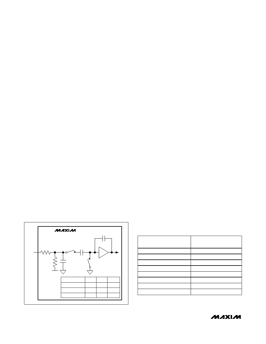
preserved. Figure 2 shows a simplified equivalent input
circuit, illustrating the ADC’s sampling architecture.
Input Bandwidth
The input tracking circuitry has a 12MHz small-signal
bandwidth, making it is possible to digitize high-speed
transient events and measure periodic signals with
bandwidths exceeding the ADC’s sampling rate by using
undersampling techniques. To avoid high-frequency
signals being aliased into the frequency band of interest,
anti-alias filtering is recommended.
Input Range and Protection
These devices provide ±10V, ±5V, or 0 to +5V analog
input voltage ranges. Figure 2 shows the equivalent input
circuit. Overvoltage protection circuitry at the analog
input provides ±16.5V fault protection for the bipolar input
devices and ±6.0V fault protection for the unipolar input
devices. This fault-protection circuit limits the current
going into or out of the device to less than 50mA, provid-
ing an added layer of protection from momentary over-
voltage or undervoltage conditions at the analog input.
Power-Saving Modes
Shutdown Mode
During shutdown, the analog and digital circuits in the
device power down and the device draws less than
100A from AVDD, and less than 100A from DVDD.
Select shutdown mode using the SHDN input. Set SHDN
high to enter shutdown mode. After coming out of shut-
down, allow a 1ms wake-up time before making the first
conversion. When using an external clock, apply at least
20 clock cycles with CONVST high before making the first
conversion. When using internal-clock mode, wait at least
2s before making the first conversion.
ALLON
ALLON is useful when some of the analog input channels
are selected (see the
Configuration Register section).
Drive ALLON high to power up all input channel circuits,
regardless of whether they are selected as active by the
configuration register. Drive ALLON low or connect to
ground to power only the input channels selected as
active by the configuration register, saving 2mA per
channel (typ). The wake-up time for any channel turned
on with the configuration register is 2s (typ) when
ALLON is low. The wake-up time with ALLON high is
only 0.01s. New configuration-register information
does not become active until the next CONVST falling
edge. Therefore, when using software to control power
states (ALLON = 0), pulse CONVST low once before
applying the actual CONVST signal (Figure 3). With an
external clock, apply at least 15 clock cycles before
the second CONVST. If using internal-clock mode, wait
at least 1.5s or until the first EOC before generating
the second CONVST.
Figure 2. Typical Input Circuit
CH_
R1
R2
VBIAS
CPAR
1pF
5pF
MAX1316–MAX1318
MAX1320–MAX1322
MAX1324–MAX1326
INPUT RANGE (V)
0 TO +5
±5
±10
R1 (k)
3.33
6.67
13.33
R2 (k)
5.00
2.86
2.35
VBIAS (V)
0.90
2.50
2.06
Table 1. Conversion Times Using the
Internal Clock
NUMBER OF CHANNELS
INTERNAL-CLOCK
CONVERSION TIME
1
1.6
2
1.9
3
2.2
4
2.5
5
2.8
6
3.1
7
3.4
8
3.7
相关PDF资料 |
PDF描述 |
|---|---|
| MAX1144BEAP+ | IC ADC 14BIT 150KSPS 20-SSOP |
| TMK316B7475KL-T | CAP CER 4.7UF 25V 10% X7R 1206 |
| MAX176ACPA+ | IC ADC 12BIT 250KSPS 8-DIP |
| VE-B5Z-IU-F3 | CONVERTER MOD DC/DC 2V 80W |
| MAX194BCWE+ | IC ADC 14BIT 85KSPS SHTDN 16SOIC |
相关代理商/技术参数 |
参数描述 |
|---|---|
| MAX1320ECM+ | 功能描述:模数转换器 - ADC 14-Bit 8Ch 526ksps 3V Precision ADC RoHS:否 制造商:Texas Instruments 通道数量:2 结构:Sigma-Delta 转换速率:125 SPs to 8 KSPs 分辨率:24 bit 输入类型:Differential 信噪比:107 dB 接口类型:SPI 工作电源电压:1.7 V to 3.6 V, 2.7 V to 5.25 V 最大工作温度:+ 85 C 安装风格:SMD/SMT 封装 / 箱体:VQFN-32 |
| MAX1320ECM+T | 功能描述:模数转换器 - ADC 14-Bit 8Ch 526ksps 3V Precision ADC RoHS:否 制造商:Texas Instruments 通道数量:2 结构:Sigma-Delta 转换速率:125 SPs to 8 KSPs 分辨率:24 bit 输入类型:Differential 信噪比:107 dB 接口类型:SPI 工作电源电压:1.7 V to 3.6 V, 2.7 V to 5.25 V 最大工作温度:+ 85 C 安装风格:SMD/SMT 封装 / 箱体:VQFN-32 |
| MAX1320ECM-T | 功能描述:模数转换器 - ADC RoHS:否 制造商:Texas Instruments 通道数量:2 结构:Sigma-Delta 转换速率:125 SPs to 8 KSPs 分辨率:24 bit 输入类型:Differential 信噪比:107 dB 接口类型:SPI 工作电源电压:1.7 V to 3.6 V, 2.7 V to 5.25 V 最大工作温度:+ 85 C 安装风格:SMD/SMT 封装 / 箱体:VQFN-32 |
| MAX1320EVB16 | 功能描述:数据转换 IC 开发工具 8-/4-/2-Channel 14-Bit Simultaneous-Sampling ADCs with 10V 5V and 0 to +5V Analog Input Ranges RoHS:否 制造商:Texas Instruments 产品:Demonstration Kits 类型:ADC 工具用于评估:ADS130E08 接口类型:SPI 工作电源电压:- 6 V to + 6 V |
| MAX1320EVKIT | 功能描述:数据转换 IC 开发工具 Evaluation Kit/Evaluation System for the MAX1316 MAX1317 MAX1318 MAX1319 MAX1320 MAX1321 MAX1322 RoHS:否 制造商:Texas Instruments 产品:Demonstration Kits 类型:ADC 工具用于评估:ADS130E08 接口类型:SPI 工作电源电压:- 6 V to + 6 V |
发布紧急采购,3分钟左右您将得到回复。