- 您现在的位置:买卖IC网 > PDF目录1936 > MAX13431EEUB+T (Maxim Integrated Products)TXRX RS-485 16MBPS HALF 10MSOP PDF资料下载
参数资料
| 型号: | MAX13431EEUB+T |
| 厂商: | Maxim Integrated Products |
| 文件页数: | 12/20页 |
| 文件大小: | 0K |
| 描述: | TXRX RS-485 16MBPS HALF 10MSOP |
| 产品培训模块: | Lead (SnPb) Finish for COTS Obsolescence Mitigation Program |
| 标准包装: | 2,500 |
| 类型: | 收发器 |
| 驱动器/接收器数: | 1/1 |
| 规程: | RS485 |
| 电源电压: | 3 V ~ 5.5 V |
| 安装类型: | 表面贴装 |
| 封装/外壳: | 10-TFSOP,10-MSOP(0.118",3.00mm 宽) |
| 供应商设备封装: | 10-µMAX |
| 包装: | 带卷 (TR) |
RS-485 Transceivers with Low-Voltage
Logic Interface
ABSOLUTE MAXIMUM RATINGS
DC ELECTRICAL CHARACTERISTICS
(VCC = +3V to +5.5V, VL = +1.8V to VCC, TA = -40°C to +85°C, unless otherwise noted. Typical values are VCC = +5V, VL = +1.8V at
TA = +25°C.) (Notes 2, 3)
Stresses beyond those listed under “Absolute Maximum Ratings” may cause permanent damage to the device. These are stress ratings only, and functional
operation of the device at these or any other conditions beyond those indicated in the operational sections of the specifications is not implied. Exposure to
absolute maximum rating conditions for extended periods may affect device reliability.
Note 1: Package thermal resistances were obtained using the method described in JEDEC specification JESD51-7, using a four-
layer board. For detailed information on package thermal considerations, refer to www.maxim-ic.com/thermal-tutorial.
(All voltages referenced to GND.)
Supply Voltage (VCC) ...............................................-0.3V to +6V
Logic Supply Voltage (VL ) ......................................-0.3V to +6V
Control Input Voltage (RE) .............................-0.3V to (VL+0.3V)
Control Input Voltage (DE) ......................................-0.3V to +6V
Driver Input Voltage (DI) ..........................................-0.3V to +6V
Driver Output Voltage (Y, Z, A, B) ............................-8V to +13V
Receiver Input Voltage (A, B)
(MAX13430E/MAX13431E)....................................-8V to +13V
Receiver Input Voltage (A, B)
(MAX13432E/MAX13433E)..................................-25V to +25V
Receiver Output Voltage (RO) .....................-0.3V to (VL + 0.3V)
Driver Output Current ....................................................±250mA
Short-Circuit Duration (RO, A, B) to GND .................Continuous
Power Dissipation (TA = +70°C)
10-Pin MAX (derate 8.8mW/°C above +70°C) ..........707mW
10-Pin TDFN (derate 24.4mW/°C above +70°C) ......1951mW
14-Pin TDFN (derate 24.4mW/°C above +70°C) ......1951mW
14-Pin SO (derate 11.9mW/°C above +70°C) .............952mW
Junction-to-Ambient Thermal Resistance (
θJA) (Note 1)
10-Pin MAX ...........................................................113.1°C/W
10-Pin TDFN .................................................................41°C/W
14-Pin TDFN ................................................................41°C/W
14-Pin SO ....................................................................84°C/W
Junction-to-Ambient Thermal Resistance (
θJC) (Note 1)
10-Pin MAX ................................................................42°C/W
10-Pin TDFN ...................................................................9°C/W
14-Pin TDFN ..................................................................8°C/W
14-Pin SO ....................................................................34°C/W
Operating Temperature Range ...........................-40°C to +85°C
Junction Temperature ..................................................... +150°C
Storage Temperature Range .............................-65°C to +150°C
Lead Temperature (soldering, 10s) .................................+300°C
Soldering Temperature (reflow) .......................................+260°C
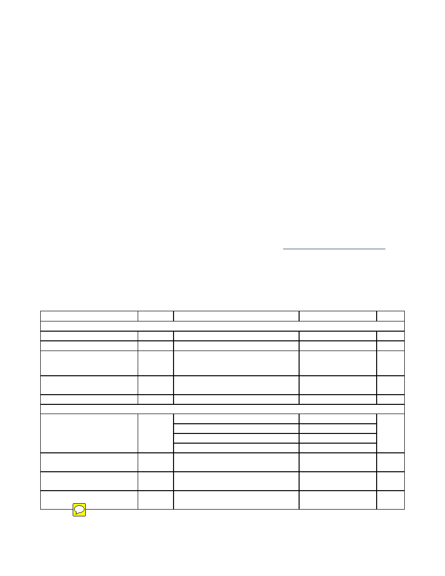
PARAMETER
SYMBOL
CONDITIONS
MIN
TYP
MAX
UNITS
POWER SUPPLY
VCC Supply-Voltage Range
VCC
3
5.5
V
VL Supply-Voltage Range
VL
1.62
VCC
V
ICC Supply Current
ICC
DE = RE = high, no load
DE = RE = low, no load
DE = high, RE = low, no load
2mA
ICC Supply Current in Shutdown
Mode
ISHDN
DE = low, RE = high, no load
10
A
VL Supply Current
IL
RO = no load
1
A
DRIVER
RL = 100
Ω, VCC = +3V
2
VCC
RL = 54
Ω, VCC = +3V
1.5
VCC
RL = 100
Ω, VCC = +4.5V
2.25
VCC
Differential Driver Output
(Figure 1)
VOD
RL = 54
Ω, VCC = +4.5V
2.25
VCC
V
Change in Magnitude of
Differential Output Voltage
ΔVOD
RL = 100
Ω or 54Ω, Figure 1 (Note 4)
0.2
V
Driver Common-Mode Output
Voltage
VOC
RL = 100
Ω or 54Ω, Figure 1
VCC/2
3
V
Change in Magnitude of
Common-Mode Voltage
ΔVOC
RL = 100
Ω or 54Ω, Figure 1 (Note 4)
0.2
V
MAX13430E–MAX13433E
2
Maxim Integrated
相关PDF资料 |
PDF描述 |
|---|---|
| MAX13443EASA+T | IC TXRX RS485 HALF DUPLEX 8-SOIC |
| MAX13448EESD+T | IC TXRX RS485 FULL DUPLEX 14SOIC |
| MAX13450EAUD+ | TXRX RS-485 14TSSOP |
| MAX13482EETE+T | IC TXRX USB ESD PROT 16-TQFN |
| MAX13486EESA+ | IC TXRX RS485/422 8-SOIC |
相关代理商/技术参数 |
参数描述 |
|---|---|
| MAX13432EESD+ | 功能描述:RS-485接口IC Txrx RS-485 0.5Mbps Full RoHS:否 制造商:Texas Instruments 数据速率:250 Kbps 工作电源电压:3.3 V 电源电流:750 uA 工作温度范围:- 40 C to + 125 C 安装风格:SMD/SMT 封装 / 箱体:SOIC-8 封装:Tube |
| MAX13432EESD+T | 功能描述:RS-485接口IC Txrx RS-485 0.5Mbps Full RoHS:否 制造商:Texas Instruments 数据速率:250 Kbps 工作电源电压:3.3 V 电源电流:750 uA 工作温度范围:- 40 C to + 125 C 安装风格:SMD/SMT 封装 / 箱体:SOIC-8 封装:Tube |
| MAX13432EETD+ | 制造商:Maxim Integrated Products 功能描述:LINE TRNSCVR 1TR 1TX 1RX 14TDFN EP - Rail/Tube |
| MAX13432EETD+T | 功能描述:RS-485接口IC Txrx RS-485 0.5Mbps Full RoHS:否 制造商:Texas Instruments 数据速率:250 Kbps 工作电源电压:3.3 V 电源电流:750 uA 工作温度范围:- 40 C to + 125 C 安装风格:SMD/SMT 封装 / 箱体:SOIC-8 封装:Tube |
| MAX13433EESD/V+ | 功能描述:RS-485接口IC RS-485 Transceivers with Low-Voltage Logic Interface RoHS:否 制造商:Texas Instruments 数据速率:250 Kbps 工作电源电压:3.3 V 电源电流:750 uA 工作温度范围:- 40 C to + 125 C 安装风格:SMD/SMT 封装 / 箱体:SOIC-8 封装:Tube |
发布紧急采购,3分钟左右您将得到回复。