- 您现在的位置:买卖IC网 > PDF目录9466 > MAX1343BETX+T (Maxim Integrated Products)IC ADC/DAC 12BIT W/FIFO 36WQFN PDF资料下载
参数资料
| 型号: | MAX1343BETX+T |
| 厂商: | Maxim Integrated Products |
| 文件页数: | 8/44页 |
| 文件大小: | 0K |
| 描述: | IC ADC/DAC 12BIT W/FIFO 36WQFN |
| 产品培训模块: | Lead (SnPb) Finish for COTS Obsolescence Mitigation Program |
| 标准包装: | 2,500 |
| 类型: | ADC,DAC |
| 分辨率(位): | 12 b |
| 采样率(每秒): | 225k |
| 数据接口: | MICROWIRE?,QSPI?,串行,SPI? |
| 电压电源: | 模拟和数字 |
| 电源电压: | 2.7 V ~ 5.25 V |
| 工作温度: | -40°C ~ 85°C |
| 安装类型: | 表面贴装 |
| 封装/外壳: | 36-WFQFN 裸露焊盘 |
| 供应商设备封装: | 36-TQFN 裸露焊盘(6x6) |
| 包装: | 带卷 (TR) |
第1页第2页第3页第4页第5页第6页第7页当前第8页第9页第10页第11页第12页第13页第14页第15页第16页第17页第18页第19页第20页第21页第22页第23页第24页第25页第26页第27页第28页第29页第30页第31页第32页第33页第34页第35页第36页第37页第38页第39页第40页第41页第42页第43页第44页
MAX1221/MAX1223/MAX1343
12-Bit, Multichannel ADCs/DACs with FIFO,
Temperature Sensing, and GPIO Ports
16
______________________________________________________________________________________
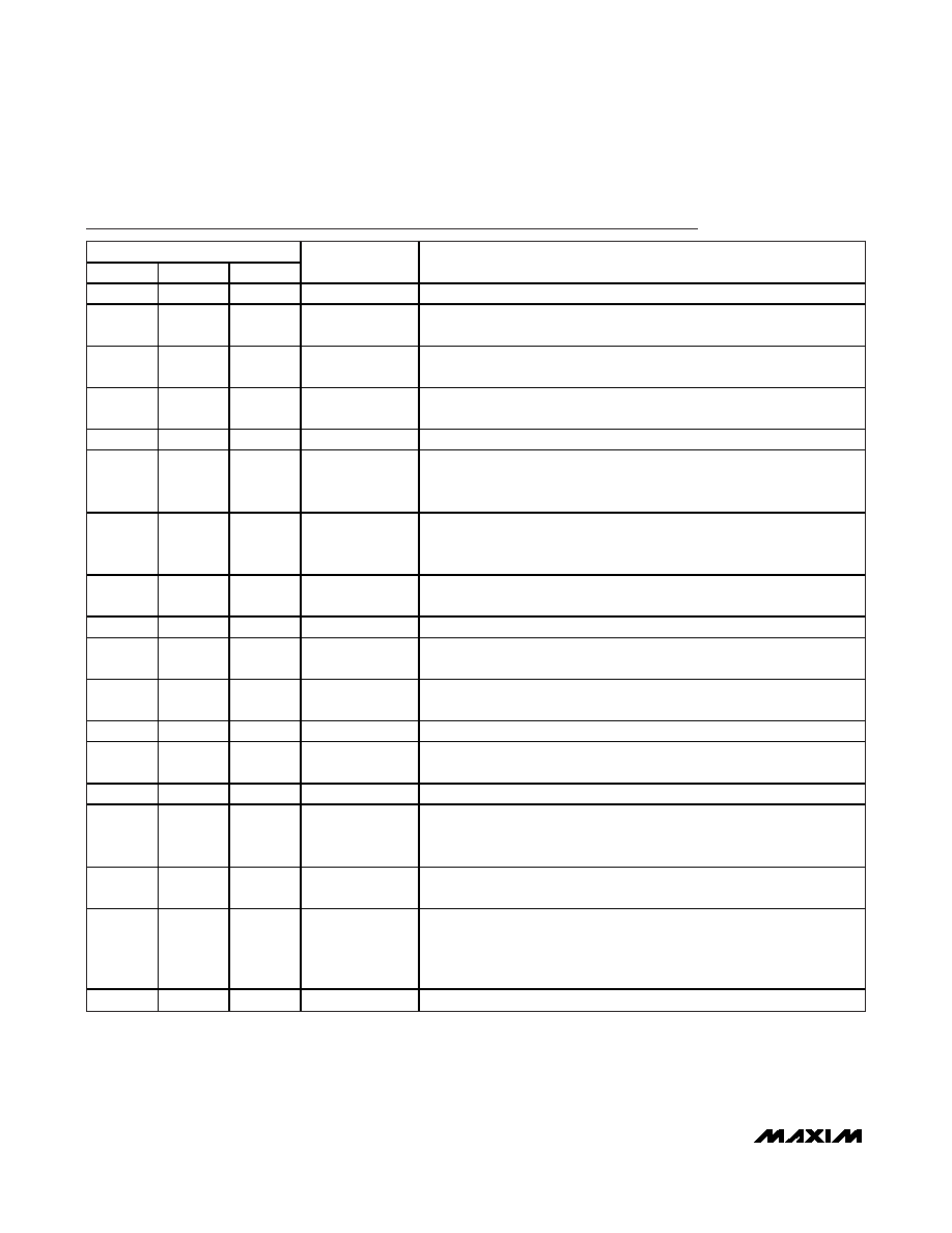
Pin Description
PIN
MAX1221
MAX1223
MAX1343
NAME
FUNCTION
1, 2
—
1, 2
GPIOA0, GPIOA1
General-Purpose I/O A0, A1. GPIOA0, A1 can sink and source 15mA.
—1
—
CNVST/AIN11
Active-Low Conversion-Start Input/Analog Input 11. See Table 5 for details
on programming the setup register.
33
3
EOC
Active-Low End-of-Conversion Output. Data is valid after the falling edge
of EOC.
44
4
DVDD
Digital Positive-Power Input. Bypass DVDD to DGND with a 0.1F
capacitor.
5
DGND
Digital Ground. Connect DGND to AGND.
6
DOUT
Serial-Data Output. Data is clocked out on the falling edge of the SCLK
clock in modes 00, 01, and 10. Data is clocked out on the rising edge of
the SCLK clock in mode 11. It is high impedance when CS is high.
7
SCLK
Serial-Clock Input. Clocks data in and out of the serial interface. (Duty
cycle must be 40% to 60%). See Table 5 for details on programming the
clock mode.
8
DIN
Serial-Data Input. DIN data is latched into the serial interface on the falling
edge of SCLK.
—
9–12
OUT0–OUT3
DAC Outputs
9–12,
16–19
9–12,
16–19
—
OUT0–OUT7
DAC Outputs
13
AVDD
Positive Analog Power Input. Bypass AVDD to AGND with a 0.1F
capacitor.
14
AGND
Analog Ground
15, 23,
32, 33
2, 15, 24,
32
15, 23,
32, 33
N.C.
No Connection. Not internally connected.
—
16–19
D.C.
Do Not Connect. Do not connect to this pin.
20
LDAC
Active-Low Load DAC. LDAC is an asynchronous active-low input that
updates the DAC outputs. Drive LDAC low to make the DAC registers
transparent.
21
CS
Active-Low Chip-Select Input. When CS is low, the serial interface is
enabled. When CS is high, DOUT is high impedance.
22
RES_SEL
Reset Select. Select DAC wake-up mode. Set RES_SEL low to wake up
the DAC outputs with a 100k
Ω resistor to GND or set RES_SEL high to
wake up the DAC outputs with a 100k
Ω resistor to VREF. The default is the
external VREF.
24, 25
—
24, 25
GPIOC0, GPIOC1
General-Purpose I/O C0, C1. GPIOC0, C1 can sink 4mA and source 2mA.
相关PDF资料 |
PDF描述 |
|---|---|
| MAX1342BETX+T | IC ADC/DAC 12BIT W/FIFO 36WQFN |
| VI-21Y-MW-S | CONVERTER MOD DC/DC 3.3V 66W |
| MAX127BCAI+T | IC DAS 12BIT 2-WIRE 28-SSOP |
| VI-27L-MY-S | CONVERTER MOD DC/DC 28V 50W |
| V375B28M300B3 | CONVERTER MOD DC/DC 28V 300W |
相关代理商/技术参数 |
参数描述 |
|---|---|
| MAX13442EASA | 功能描述:RS-485接口IC RoHS:否 制造商:Texas Instruments 数据速率:250 Kbps 工作电源电压:3.3 V 电源电流:750 uA 工作温度范围:- 40 C to + 125 C 安装风格:SMD/SMT 封装 / 箱体:SOIC-8 封装:Tube |
| MAX13442EASA+ | 功能描述:RS-485接口IC Half-Dplx RS-422/485 250ksps 5V LD/Rec RoHS:否 制造商:Texas Instruments 数据速率:250 Kbps 工作电源电压:3.3 V 电源电流:750 uA 工作温度范围:- 40 C to + 125 C 安装风格:SMD/SMT 封装 / 箱体:SOIC-8 封装:Tube |
| MAX13442EASA+T | 功能描述:RS-485接口IC Half-Dplx RS-422/485 250ksps 5V LD/Rec RoHS:否 制造商:Texas Instruments 数据速率:250 Kbps 工作电源电压:3.3 V 电源电流:750 uA 工作温度范围:- 40 C to + 125 C 安装风格:SMD/SMT 封装 / 箱体:SOIC-8 封装:Tube |
| MAX13442EASA-T | 功能描述:RS-485接口IC RoHS:否 制造商:Texas Instruments 数据速率:250 Kbps 工作电源电压:3.3 V 电源电流:750 uA 工作温度范围:- 40 C to + 125 C 安装风格:SMD/SMT 封装 / 箱体:SOIC-8 封装:Tube |
| MAX13443EASA | 功能描述:RS-485接口IC RoHS:否 制造商:Texas Instruments 数据速率:250 Kbps 工作电源电压:3.3 V 电源电流:750 uA 工作温度范围:- 40 C to + 125 C 安装风格:SMD/SMT 封装 / 箱体:SOIC-8 封装:Tube |
发布紧急采购,3分钟左右您将得到回复。