- 您现在的位置:买卖IC网 > PDF目录224186 > MAX1459CAP+T (MAXIM INTEGRATED PRODUCTS INC) 2-Wire, 4-20mA Smart Signal Conditioner PDF资料下载
参数资料
| 型号: | MAX1459CAP+T |
| 厂商: | MAXIM INTEGRATED PRODUCTS INC |
| 元件分类: | 模拟信号调理 |
| 英文描述: | 2-Wire, 4-20mA Smart Signal Conditioner |
| 中文描述: | SPECIALTY ANALOG CIRCUIT, PDSO20 |
| 封装: | SSOP-20 |
| 文件页数: | 22/24页 |
| 文件大小: | 243K |
| 代理商: | MAX1459CAP+T |
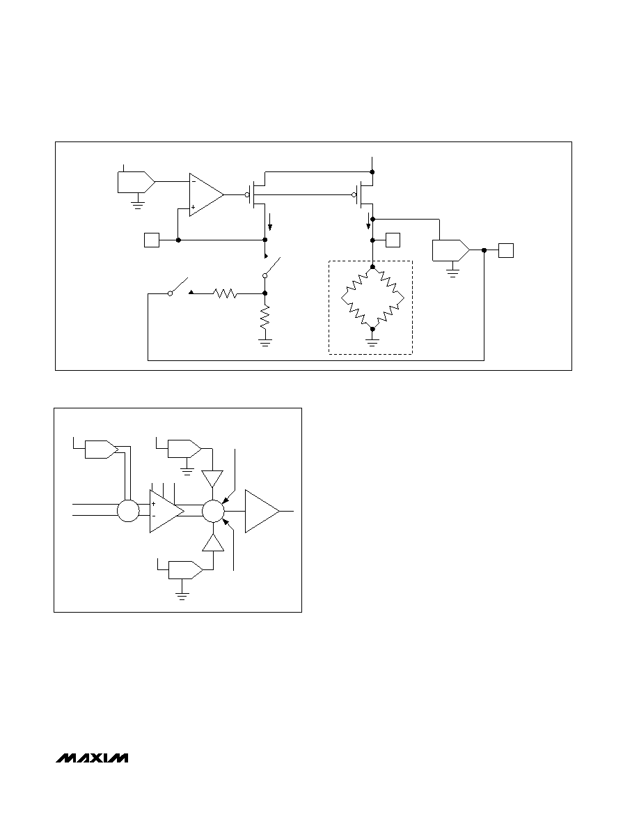
age is fed into the PGA. The 3-bit (plus sign) input-
referred offset DAC (IRO DAC) generates the coarse
offset-correction voltage. The DAC voltage reference is
1.25% of VDD; thus, a VDD of 5V results in a front-end
offset-correction voltage ranging from -63mV to +63mV,
in 9mV steps (Table 1). To add an offset to the input
signal, set the IRO sign bit high; to subtract an offset
from the input signal, set the IRO sign bit low. The IRO
DAC bits (C2, C1, C0, and IRO sign bit) are pro-
grammed in the configuration register (see Internal
EEPROM section).
Programmable-Gain Amplifier
The programmable-gain amplifier (PGA), which is used
to set the coarse FSO, uses a switched-capacitor
CMOS technology and contains eight selectable gain
levels from 41 to 230, in increments of 27 (Table 2). The
output of the PGA is fed to the output summing junc-
tion. The three PGA gain bits A2, A1, and A0 are stored
in the configuration register.
Output Summing Junction
The third stage in the analog signal path consists of a
summing junction for the PGA output, offset correction,
and the offset TC correction. Both the offset and the off-
set TC correction voltages are gained by a factor of 2.3
before being fed into the summing junction, increasing
the offset and offset TC correction range. The offset sign
bit and offset TC sign bit are stored in the configuration
register. The offset sign bit determines whether the off-
set correction voltage is added to (sign bit is high) or
subtracted from (sign bit is low) the PGA output.
Negative offset TC errors require a logic high for the off-
set TC sign bit. Alternately, positive offset TC errors dic-
tate a logic low for the offset TC sign bit. The output of
the summing junction is fed to the output buffer.
MAX1459
2-Wire, 4–20mA
Smart Signal Conditioner
_______________________________________________________________________________________
7
Figure 2. Bridge Excitation Circuit
VDD
AA
≈ 12IISRC = IBDRIVE
I = IISRC
ISRC
FSOTC
RISRC
BDRIVE
VDD
RFTC
EXTERNAL
SENSOR
FSO
DAC
FSOTC
DAC
SOTC
BDRIVE
1.25% VDD
SOFF
±
A2
INP
INM
A1 A0
PGA
Σ
A = 1
OUT
A = 2.3
OFFTC
DAC
IRO
DAC
VDD
OFFSET
DAC
Figure 3. Signal-Path Block Diagram
相关PDF资料 |
PDF描述 |
|---|---|
| MAX1459AAP+T | 2-Wire, 4-20mA Smart Signal Conditioner |
| MAX1459CAP+ | 2-Wire, 4-20mA Smart Signal Conditioner |
| MAX1459AAP+ | 2-Wire, 4-20mA Smart Signal Conditioner |
| MAX147BEAP+ | +2.7V, Low-Power, 8-Channel, Serial 12-Bit ADCs |
| MAX147BEAP+T | +2.7V, Low-Power, 8-Channel, Serial 12-Bit ADCs |
相关代理商/技术参数 |
参数描述 |
|---|---|
| MAX145ACPA | 功能描述:模数转换器 - ADC RoHS:否 制造商:Texas Instruments 通道数量:2 结构:Sigma-Delta 转换速率:125 SPs to 8 KSPs 分辨率:24 bit 输入类型:Differential 信噪比:107 dB 接口类型:SPI 工作电源电压:1.7 V to 3.6 V, 2.7 V to 5.25 V 最大工作温度:+ 85 C 安装风格:SMD/SMT 封装 / 箱体:VQFN-32 |
| MAX145ACPA+ | 功能描述:模数转换器 - ADC 12-Bit 108ksps 5.25V High Speed ADC RoHS:否 制造商:Texas Instruments 通道数量:2 结构:Sigma-Delta 转换速率:125 SPs to 8 KSPs 分辨率:24 bit 输入类型:Differential 信噪比:107 dB 接口类型:SPI 工作电源电压:1.7 V to 3.6 V, 2.7 V to 5.25 V 最大工作温度:+ 85 C 安装风格:SMD/SMT 封装 / 箱体:VQFN-32 |
| MAX145ACUA | 功能描述:模数转换器 - ADC RoHS:否 制造商:Texas Instruments 通道数量:2 结构:Sigma-Delta 转换速率:125 SPs to 8 KSPs 分辨率:24 bit 输入类型:Differential 信噪比:107 dB 接口类型:SPI 工作电源电压:1.7 V to 3.6 V, 2.7 V to 5.25 V 最大工作温度:+ 85 C 安装风格:SMD/SMT 封装 / 箱体:VQFN-32 |
| MAX145ACUA+ | 功能描述:模数转换器 - ADC 12-Bit 108ksps 5.25V High Speed ADC RoHS:否 制造商:Texas Instruments 通道数量:2 结构:Sigma-Delta 转换速率:125 SPs to 8 KSPs 分辨率:24 bit 输入类型:Differential 信噪比:107 dB 接口类型:SPI 工作电源电压:1.7 V to 3.6 V, 2.7 V to 5.25 V 最大工作温度:+ 85 C 安装风格:SMD/SMT 封装 / 箱体:VQFN-32 |
| MAX145ACUA+T | 功能描述:模数转换器 - ADC 12-Bit 108ksps 5.25V High Speed ADC RoHS:否 制造商:Texas Instruments 通道数量:2 结构:Sigma-Delta 转换速率:125 SPs to 8 KSPs 分辨率:24 bit 输入类型:Differential 信噪比:107 dB 接口类型:SPI 工作电源电压:1.7 V to 3.6 V, 2.7 V to 5.25 V 最大工作温度:+ 85 C 安装风格:SMD/SMT 封装 / 箱体:VQFN-32 |
发布紧急采购,3分钟左右您将得到回复。