- 您现在的位置:买卖IC网 > PDF目录1936 > MAX14806CCM+T (Maxim Integrated Products)IC MUX DUAL 8CH HV 48LQFP PDF资料下载
参数资料
| 型号: | MAX14806CCM+T |
| 厂商: | Maxim Integrated Products |
| 文件页数: | 7/14页 |
| 文件大小: | 0K |
| 描述: | IC MUX DUAL 8CH HV 48LQFP |
| 应用说明: | Ultrasound Imaging Systems Application Note |
| 产品培训模块: | Lead (SnPb) Finish for COTS Obsolescence Mitigation Program |
| 标准包装: | 2,000 |
| 功能: | 开关 |
| 电路: | 8 x SPST - NO,8 x SPST - NC |
| 导通状态电阻: | 23 欧姆 |
| 电压电源: | 单电源 |
| 电压 - 电源,单路/双路(±): | 2.7 V ~ 5.5 V |
| 工作温度: | -40°C ~ 85°C |
| 安装类型: | 表面贴装 |
| 封装/外壳: | 48-LQFP |
| 供应商设备封装: | 48-LQFP(7x7) |
| 包装: | 带卷 (TR) |
2 ______________________________________________________________________________________
MAX14805/MAX14806
16-Channel (Two Banks of 8-Channel),
High-Voltage Analog Switches
Stresses beyond those listed under “Absolute Maximum Ratings” may cause permanent damage to the device. These are stress ratings only, and functional
operation of the device at these or any other conditions beyond those indicated in the operational sections of the specifications is not implied. Exposure to absolute
maximum rating conditions for extended periods may affect device reliability.
(All voltages referenced to GND.)
VDD Logic Supply Voltage ......................................-0.3V to +7V
VPP - VNN Supply Voltage ..................................................230V
VPP Positive Supply Voltage ..............................-0.3V to +220V
VNN Negative Supply Voltage ............................+0.3V to -220V
Logic Inputs Voltage (LE, DIN1, DIN2) ..................-0.3V to +7V
Analog Signal Range (SW_).......(-0.3V + VNN) to (VNN + 200V)
Peak Analog Signal Current per Channel ..............................3A
Continuous Power Dissipation (TA = +70NC)
48-Pin TQFP (derate 22.7mW/NC above +70NC) ......1818mW
Junction-to-Ambient Thermal Resistance
B
JA (Note 1) .................................................................44NC/W
Junction-to-Case Thermal Resistance
B
JC (Note 1) ................................................................10NC/W
Operating Temperature Range.......................... -40NC to +85NC
Storage Temperature Range............................ -65NC to +150NC
Junction Temperature ................................................... +150NC
Lead Temperature (soldering, 10s) ................................+300NC
Soldering Temperature (reflow) ......................................+260NC
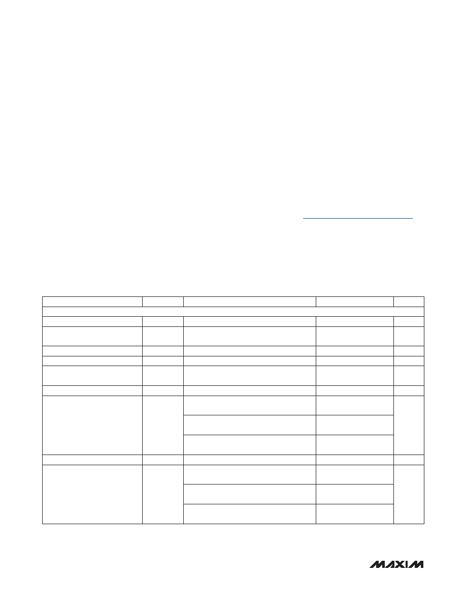
ELECTRICAL CHARACTERISTICS
(VDD = +2.7V to +5.5V, VPP = +40V to (VNN + 200V), VNN = -40V to -160V, TA = TMIN to TMAX, unless otherwise noted. Typical
values are at TA = +25NC.) (Note 2)
ABSOLUTE MAXIMUM RATINGS
Note 1: Package thermal resistances were obtained using the method described in JEDEC specification JESD51-7, using a four-
layer board. For detailed information on package thermal considerations, refer to www.maxim-ic.com/thermal-tutorial.
PARAMETER
SYMBOL
CONDITIONS
MIN
TYP
MAX
UNITS
POWER SUPPLIES
VDD Supply Voltage
VDD
2.7
5.5
V
VPP Supply Voltage
VPP
40
100
VNN
+ 220
V
VNN Supply Voltage
VNN
-160
-100
-15
V
VDD Supply Quiescent Current
IDDQ
5
F
A
VDD Supply Dynamic Current
IDDD
VDD = +5V, LE = GND, fDIN1 = fDIN2 =
5MHz
2
mA
VPP Supply Quiescent Current
IPPQ
10
F
A
VPP Supply Dynamic Current
(All Channel Switching
Simultaneously)
IPPD
VPP = +40V, VNN = -160V, fSW_ = 50kHz,
fDIN1 = fDIN2 = 50kHz, LE = GND
5
mA
VPP = +100V, VNN = -100V, fSW_ = 50kHz,
fDIN1 = fDIN2 = 50kHz, LE = GND
6
VPP = +160V, VNN = -40V, fSW_ = 50kHz,
fDIN1 = fDIN2 = 50kHz, LE = GND
7
VNN Supply Quiescent Current
INNQ
10
F
A
VNN Supply Dynamic Current
(All Channel Switching
Simultaneously)
INND
VPP = +40V, VNN = -160V, fSW_ = 50kHz,
fDIN1 = fDIN2 = 50kHz, LE = GND
5.5
mA
VPP = +100V, VNN = -100V, fSW_ = 50kHz,
fDIN1 = fDIN2 = 50kHz, LE = GND
5
VPP = +160V, VNN = -40V, fSW_ = 50kHz,
fDIN1 = fDIN2 = 50kHz, LE = GND
4.5
相关PDF资料 |
PDF描述 |
|---|---|
| MAX1480CEPI+ | IC INTERFACE RS485/RS422 28-DIP |
| MAX1480ECEPI+ | IC RS485/RS422 DATA INTRFC 28DIP |
| MAX14820ETG+ | IC IO-LINK TXRX 24TQFN |
| MAX14821ETG+ | IC IO-LINK 24-TQFN |
| MAX14824GTG+ | IC IO-LINK MASTER TXRX 24TQFN |
相关代理商/技术参数 |
参数描述 |
|---|---|
| MAX14806ECM+ | 功能描述:模拟开关 IC 8:1 2Ch High Voltage A Switch w/Bleed Res RoHS:否 制造商:Texas Instruments 开关数量:2 开关配置:SPDT 开启电阻(最大值):0.1 Ohms 切换电压(最大): 开启时间(最大值): 关闭时间(最大值): 工作电源电压:2.7 V to 4.5 V 最大工作温度:+ 85 C 安装风格:SMD/SMT 封装 / 箱体:DSBGA-16 |
| MAX14808ETK+T | 制造商:Maxim Integrated Products 功能描述:OCTAL THREE-LEVEL/QUAD FIVE-LEVEL HIGH-VOLTAGE 2A DIGITAL PU - Tape and Reel |
| MAX14809ETK+T | 制造商:Maxim Integrated Products 功能描述:OCTAL HV DIGITAL PULSER - Tape and Reel |
| MAX1480ACPI | 功能描述:RS-422/RS-485 接口 IC RoHS:否 制造商:Maxim Integrated 数据速率:1136 Kbps 工作电源电压:3 V to 5.5 V 电源电流:5.9 mA 工作温度范围:- 40 C to + 85 C 安装风格:SMD/SMT 封装 / 箱体:SOIC-28 封装:Tube |
| MAX1480ACPI+ | 功能描述:RS-422/RS-485 接口 IC Isolated RS-422/485 Data Interface RoHS:否 制造商:Maxim Integrated 数据速率:1136 Kbps 工作电源电压:3 V to 5.5 V 电源电流:5.9 mA 工作温度范围:- 40 C to + 85 C 安装风格:SMD/SMT 封装 / 箱体:SOIC-28 封装:Tube |
发布紧急采购,3分钟左右您将得到回复。