- 您现在的位置:买卖IC网 > PDF目录16278 > MAX14821EVKIT# (Maxim Integrated Products)EVAL KIT MAX14821 PDF资料下载
参数资料
| 型号: | MAX14821EVKIT# |
| 厂商: | Maxim Integrated Products |
| 文件页数: | 7/31页 |
| 文件大小: | 0K |
| 描述: | EVAL KIT MAX14821 |
| 产品培训模块: | Lead (SnPb) Finish for COTS Obsolescence Mitigation Program |
| 标准包装: | 1 |
| 主要目的: | 接口,收发器 |
| 已用 IC / 零件: | MAX14821 |
| 主要属性: | IO和SPI接口端子 |
| 次要属性: | 图形用户界面 |
| 已供物品: | 板,线缆,软件 |
第1页第2页第3页第4页第5页第6页当前第7页第8页第9页第10页第11页第12页第13页第14页第15页第16页第17页第18页第19页第20页第21页第22页第23页第24页第25页第26页第27页第28页第29页第30页第31页
MAX14821
IO-Link Device Transceiver
15
Maxim Integrated
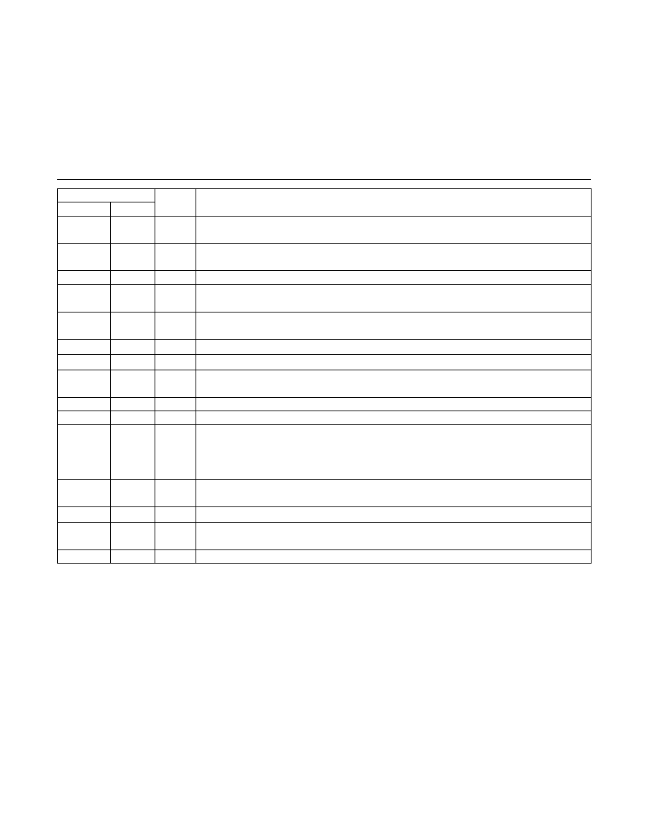
Pin/Bump Descriptions (continued)
PIN
NAME
FUNCTION
TQFN-EP
WLP
11
D5
TXQ
Transmit Level Input. The logic on the C/Q output is the inverse logic level of the signals on
the TXC and TXQ inputs. TXQ is ANDed with TXC. Drive TXQ high if not in use.
12
D4
TXC
Transmit Communication Input. The logic on the C/Q output is the inverse logic level of the
signals on the TXC and TXQ inputs. TXC is ANDed with TXQ. Drive TXC high if not in use.
13
E5
TXEN
Transmitter Enable. Drive TXEN high to enable the C/Q transmitter. TXEN is referenced to VL.
14
E4
RX
Receiver Output. RX is the inverse logic level of C/Q. RX is always high when the RxDis bit in
the CQConfig register is set to 1.
15
D3
WU
Active-Low Wake-Up Output. WU is a push-pull output referenced to VL. WU pulses low for
190Fs (typ) when a valid wake-up pulse is detected on the C/Q line.
16
E3
LO
Logic Input of the DO Output. LO is the logic input that drives DO. LO is referenced to VL.
17
E2
LI
Logic Output of the 24V DI Logic Input. LI is the inverse logic of DI. LI is referenced to VL.
18
D2
UV
Open-Drain Undervoltage Indicator Output. In case of an undervoltage, the UV open-drain
transistor is off.
19
E1
DI
24V Logic-Level Digital Input
20
C1, C2
GND
Ground
21
B1
C/Q
SIO/IO-Link Data Input/Output. Drive TXEN high to enable the C/Q driver. The logic on the
C/Q output is the inverse logic level of the signals on the TXC and TXQ inputs. RX is the logic
inverse of C/Q. The C/Q driver output level can be set by the TXC/TXQ inputs or programmed
by the Q bit. The level on C/Q can be read by the RX ouput or the QLvl bit.
22
D1
DO
24V Logic-Level Digital Output. DO is the inverse logic level of the LO input and can be digi-
tally controlled through the DIOConfig register.
23
A1
VCC
Power-Supply Input. Bypass VCC to GND with a 1FF ceramic capacitor.
24
B2
VP
Protected 24V Supply Output. VP is one diode drop below VCC. VP is reverse-polarity protect-
ed and can be used as a 24V protected supply to the sensor or actuator electronics.
—
EP
Exposed Pad (TQFN Only). Connect EP to GND.
相关PDF资料 |
PDF描述 |
|---|---|
| UVZ1C472MHD | CAP ALUM 4700UF 16V 20% RADIAL |
| 78Q2123-DB | BOARD DEMO 78Q2123 78Q2133 |
| 78Q2120C09-DB | BOARD DEMO 78Q2120C |
| NCP301LSN45T1G | IC DETECTOR VOLTAGE 4.5V 5TSOP |
| MAX810TTRG | IC MPU SUPERVISORY 3.08V SOT23 |
相关代理商/技术参数 |
参数描述 |
|---|---|
| MAX14821EVKIT# | 功能描述:界面开发工具 MAX14820/21 EVAL KIT RoHS:否 制造商:Bourns 产品:Evaluation Boards 类型:RS-485 工具用于评估:ADM3485E 接口类型:RS-485 工作电源电压:3.3 V |
| MAX14821EWA+ | 制造商:Maxim Integrated Products 功能描述:- Rail/Tube |
| MAX14821EWA+T | 功能描述:输入/输出控制器接口集成电路 100mA IO-Link Transceiver RoHS:否 制造商:Silicon Labs 产品: 输入/输出端数量: 工作电源电压: 最大工作温度:+ 85 C 最小工作温度:- 40 C 安装风格:SMD/SMT 封装 / 箱体:QFN-64 封装:Tray |
| MAX14824ETG+ | 功能描述:输入/输出控制器接口集成电路 IO-Link Master Transceiver RoHS:否 制造商:Silicon Labs 产品: 输入/输出端数量: 工作电源电压: 最大工作温度:+ 85 C 最小工作温度:- 40 C 安装风格:SMD/SMT 封装 / 箱体:QFN-64 封装:Tray |
| MAX14824ETG+T | 功能描述:输入/输出控制器接口集成电路 IO-Link Master Transceiver RoHS:否 制造商:Silicon Labs 产品: 输入/输出端数量: 工作电源电压: 最大工作温度:+ 85 C 最小工作温度:- 40 C 安装风格:SMD/SMT 封装 / 箱体:QFN-64 封装:Tray |
发布紧急采购,3分钟左右您将得到回复。