- 您现在的位置:买卖IC网 > PDF目录9902 > MAX148AEPP+ (Maxim Integrated Products)IC ADC 10BIT SERIAL 20-DIP PDF资料下载
参数资料
| 型号: | MAX148AEPP+ |
| 厂商: | Maxim Integrated Products |
| 文件页数: | 3/23页 |
| 文件大小: | 0K |
| 描述: | IC ADC 10BIT SERIAL 20-DIP |
| 产品培训模块: | Lead (SnPb) Finish for COTS Obsolescence Mitigation Program |
| 标准包装: | 18 |
| 位数: | 10 |
| 采样率(每秒): | 133k |
| 数据接口: | MICROWIRE?,QSPI?,串行,SPI? |
| 转换器数目: | 1 |
| 功率耗散(最大): | 889mW |
| 电压电源: | 单电源 |
| 工作温度: | -40°C ~ 85°C |
| 安装类型: | 通孔 |
| 封装/外壳: | 20-DIP(0.300",7.62mm) |
| 供应商设备封装: | 20-PDIP |
| 包装: | 管件 |
| 输入数目和类型: | 8 个单端,单极;8 个单端,双极;4 个差分,单极;4 个差分,双极 |
+2.7V to +5.25V, Low-Power, 8-Channel,
Serial 10-Bit ADCs
MAX148/MAX149
11
Table 3. Channel Selection in Differential Mode (SGL/DIF = 0)
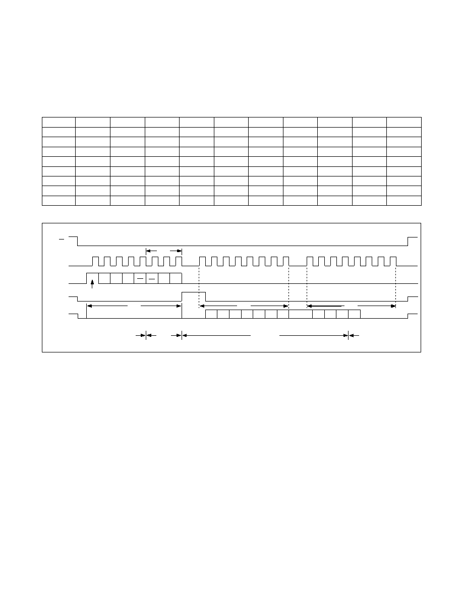
Figure 6. 24-Clock External Clock Mode Conversion Timing (MICROWIRE and SPI-Compatible, QSPI-Compatible with fSCLK P 2MHz)
Simple Software Interface
Make sure the CPU’s serial interface runs in master
mode so the CPU generates the serial clock. Choose a
clock frequency from 100kHz to 2MHz.
1) Set up the control byte for external clock mode and
call it TB1. TB1 should be of the format: 1XXXXX11
binary, where the Xs denote the particular channel
and conversion mode selected.
2) Use a general-purpose I/O line on the CPU to pull CS
low.
3) Transmit TB1 and, simultaneously, receive a byte
and call it RB1. Ignore RB1.
4) Transmit a byte of all zeros ($00 hex) and, simultane-
ously, receive byte RB2.
5) Transmit a byte of all zeros ($00 hex) and, simultane-
ously, receive byte RB3.
6) Pull CS high.
Figure 6 shows the timing for this sequence. Bytes RB2
and RB3 contain the result of the conversion, padded
with one leading zero, two sub-LSB bits, and three
trailing zeros. The total conversion time is a function of
the serial-clock frequency and the amount of idle time
between 8-bit transfers. To avoid excessive T/H droop,
make sure the total conversion time does not exceed
120Fs.
Digital Output
In unipolar input mode, the output is straight binary
(Figure 17). For bipolar input mode, the output is twos
complement (Figure 18). Data is clocked out at the fall-
ing edge of SCLK in MSB-first format.
Clock Modes
The MAX148/MAX149 may use either an external serial
clock or the internal clock to perform the successive-
approximation conversion. In both clock modes, the exter-
nal clock shifts data in and out of the MAX148/MAX149.
SEL2
SEL1
SEL0
CH0
CH1
CH2
CH3
CH4
CH5
CH6
CH7
0
+
-
0
1
+
-
0
1
0
+
-
0
1
+
-
1
0
-
+
1
0
1
-
+
1
0
-
+
1
-
+
1
4
8
12
16
20
24
START
SEL2 SEL1 SEL0
UNI/
BIP
SGL/
DIF
PD1 PD0
B9
MSB
B8
B7
B6
B5
B4
B3
B2
B1
S0
S1
B0
LSB
FILLED WITH
ZEROS
RB1
RB2
IDLE
CONVERSION
RB3
ACQUISITION
(fSCLK = 2MHz)
IDLE
1.5Fs
SCLK
tACQ
DIN
SSTRB
DOUT
A/D STATE
CS
相关PDF资料 |
PDF描述 |
|---|---|
| IDT72V36100L7-5BB | IC FIFO 64X36 7-5NS 144BGA |
| MAX1067BCEE+T | IC ADC 14BIT 200KSPS 16-QSOP |
| V48A28T500BG | CONVERTER MOD DC/DC 28V 500W |
| IDT72V2103L7-5BC | IC FIFO SUPERSYNCII 7-5NS 100BGA |
| MAX139CMH+TD | IC ADC 3.5 DIG W/LED DVR 44MQFP |
相关代理商/技术参数 |
参数描述 |
|---|---|
| MAX148AEPP+ | 功能描述:模数转换器 - ADC 10-Bit 8Ch 133ksps 5.25V Precision ADC RoHS:否 制造商:Texas Instruments 通道数量:2 结构:Sigma-Delta 转换速率:125 SPs to 8 KSPs 分辨率:24 bit 输入类型:Differential 信噪比:107 dB 接口类型:SPI 工作电源电压:1.7 V to 3.6 V, 2.7 V to 5.25 V 最大工作温度:+ 85 C 安装风格:SMD/SMT 封装 / 箱体:VQFN-32 |
| MAX148AMJP | 功能描述:模数转换器 - ADC RoHS:否 制造商:Texas Instruments 通道数量:2 结构:Sigma-Delta 转换速率:125 SPs to 8 KSPs 分辨率:24 bit 输入类型:Differential 信噪比:107 dB 接口类型:SPI 工作电源电压:1.7 V to 3.6 V, 2.7 V to 5.25 V 最大工作温度:+ 85 C 安装风格:SMD/SMT 封装 / 箱体:VQFN-32 |
| MAX148BC/D | 功能描述:模数转换器 - ADC +2.7V to +5.25V Low-Power 8-Channel Serial 10-Bit ADCs RoHS:否 制造商:Texas Instruments 通道数量:2 结构:Sigma-Delta 转换速率:125 SPs to 8 KSPs 分辨率:24 bit 输入类型:Differential 信噪比:107 dB 接口类型:SPI 工作电源电压:1.7 V to 3.6 V, 2.7 V to 5.25 V 最大工作温度:+ 85 C 安装风格:SMD/SMT 封装 / 箱体:VQFN-32 |
| MAX148BCAP | 功能描述:模数转换器 - ADC RoHS:否 制造商:Texas Instruments 通道数量:2 结构:Sigma-Delta 转换速率:125 SPs to 8 KSPs 分辨率:24 bit 输入类型:Differential 信噪比:107 dB 接口类型:SPI 工作电源电压:1.7 V to 3.6 V, 2.7 V to 5.25 V 最大工作温度:+ 85 C 安装风格:SMD/SMT 封装 / 箱体:VQFN-32 |
| MAX148BCAP+ | 功能描述:模数转换器 - ADC 10-Bit 8Ch 133ksps 5.25V Precision ADC RoHS:否 制造商:Texas Instruments 通道数量:2 结构:Sigma-Delta 转换速率:125 SPs to 8 KSPs 分辨率:24 bit 输入类型:Differential 信噪比:107 dB 接口类型:SPI 工作电源电压:1.7 V to 3.6 V, 2.7 V to 5.25 V 最大工作温度:+ 85 C 安装风格:SMD/SMT 封装 / 箱体:VQFN-32 |
发布紧急采购,3分钟左右您将得到回复。