- 您现在的位置:买卖IC网 > PDF目录20230 > MAX1491CAI+ (Maxim Integrated)IC ADC 3.5 DGT LCD DVR 28-SSOP PDF资料下载
参数资料
| 型号: | MAX1491CAI+ |
| 厂商: | Maxim Integrated |
| 文件页数: | 4/25页 |
| 文件大小: | 0K |
| 描述: | IC ADC 3.5 DGT LCD DVR 28-SSOP |
| 产品培训模块: | Lead (SnPb) Finish for COTS Obsolescence Mitigation Program |
| 标准包装: | 46 |
| 显示器类型: | LCD |
| 配置: | 7 段 + 2 个信号器 |
| 数字或字符: | A/D,3.5 位数字 |
| 电流 - 电源: | 980µA |
| 电源电压: | 2.7 V ~ 5.25 V |
| 工作温度: | 0°C ~ 70°C |
| 安装类型: | 表面贴装 |
| 封装/外壳: | 28-SSOP(0.209",5.30mm 宽) |
| 供应商设备封装: | 28-SSOP |
| 包装: | 管件 |
| 产品目录页面: | 1397 (CN2011-ZH PDF) |
�� �
�
�3.5-� and� 4.5-Digit,� Single-Chip�
�ADCs� with� LCD� Drivers�
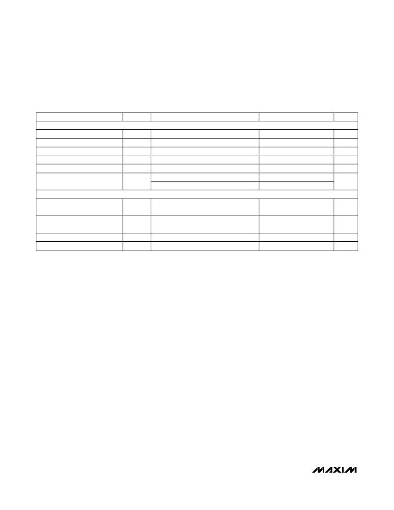
�ELECTRICAL� CHARACTERISTICS� (continued)�
�(AV� DD� =� DV� DD� =� +2.7V� to� +5.25V,� GND� =� 0,� V� REF+� -� V� REF-� =� 2.048V� (external� reference),� C� NEG� =� 0.1μF.� All� specifications� are� T� MIN�
�to� T� MAX� ,� unless� otherwise� noted.� Typical� values� are� at� +25°C,� unless� otherwise� noted.)�
�PARAMETER�
�SYMBOL�
�CONDITIONS�
�MIN�
�TYP�
�MAX�
�UNITS�
�POWER� SUPPLY�
�AV� DD� Voltage�
�DV� DD� Voltage�
�Power-Supply� Rejection� AV� DD�
�Power-Supply� Rejection� DV� DD�
�AV� DD� Current�
�DV� DD� Current�
�AV� DD�
�DV� DD�
�PSRR� A�
�PSRR� D�
�I� AVDD�
�I� DVDD�
�(Note� 7)�
�(Note� 7)�
�(Note� 8)�
�DV� DD� =� 5V�
�DV� DD� =� 3.3V�
�2.70�
�2.70�
�80�
�100�
�5.25�
�5.25�
�660�
�320�
�180�
�V�
�V�
�dB�
�dB�
�μA�
�μA�
�LCD� DRIVER�
�RMS� Segment-On� Voltage�
�RMS� Segment-Off� Voltage�
�Display� Multiplex� Rate�
�LCD� Data-Update� Rate�
�1.92� x�
�DV� DD�
�1/3x�
�DV� DD�
�107�
�2.5�
�V�
�V�
�Hz�
�Hz�
�Note� 1:� Integral� nonlinearity� is� the� derivation� of� the� analog� values� at� any� code� from� its� theoretical� value� after� nulling� the� gain� error�
�and� offset� error.�
�Note� 2:� Offset� calibrated.�
�Note� 3:� Offset� nulled.�
�Note� 4:� The� input� voltage� range� for� the� analog� inputs� is� given� with� respect� to� the� voltage� on� the� negative� input� of� the� differential� pair.�
�Note� 5:� For� the� range� of� V� AIN+� or� V� AIN-� =� -2.2V� to� +2.2V� and� V� REF+� or� V� REF-� =� -2.2V� to� +2.2V.�
�Note� 6:� External� load� must� be� constant� during� conversion� for� specified� accuracy.� Guaranteed� specification� of� 2mV/mA� is� a� result� of�
�production� test� limitations.�
�Note� 7:� Measured� at� DC� by� changing� the� power-supply� voltage� from� 2.7V� to� 5.25V� and� measuring� its� effect� on� the� conversion� error.�
�PSRR� at� 50Hz� and� 60Hz� exceeds� 120dB� with� filter� notches� of� 10,� 20,� 30,� 40,� 50,� or� 60Hz.�
�Note� 8:� Analog� power-supply� currents� are� measured� with� all� digital� inputs� at� either� GND� or� DV� DD� .� Digital� power-supply� currents�
�measured� with� all� digital� inputs� at� either� GND� or� DV� DD� .�
�4�
�_______________________________________________________________________________________�
�相关PDF资料 |
PDF描述 |
|---|---|
| 5-147490-5 | CONN CARDEDGE 55DL POS .100 GOLD |
| VI-2W1-EV-F1 | CONVERTER MOD DC/DC 12V 150W |
| VI-J31-CX-B1 | CONVERTER MOD DC/DC 12V 75W |
| RGZ-1209D/P | CONV DC/DC 2W 12VIN +/-09VOUT |
| VE-2WW-EV-F4 | CONVERTER MOD DC/DC 5.5V 150W |
相关代理商/技术参数 |
参数描述 |
|---|---|
| MAX1491CAI+ | 功能描述:模数转换器 - ADC 3.5 Digit ADC w/LCD Drivers RoHS:否 制造商:Texas Instruments 通道数量:2 结构:Sigma-Delta 转换速率:125 SPs to 8 KSPs 分辨率:24 bit 输入类型:Differential 信噪比:107 dB 接口类型:SPI 工作电源电压:1.7 V to 3.6 V, 2.7 V to 5.25 V 最大工作温度:+ 85 C 安装风格:SMD/SMT 封装 / 箱体:VQFN-32 |
| MAX1491CAI+T | 功能描述:模数转换器 - ADC 3.5 Digit ADC w/LCD Drivers RoHS:否 制造商:Texas Instruments 通道数量:2 结构:Sigma-Delta 转换速率:125 SPs to 8 KSPs 分辨率:24 bit 输入类型:Differential 信噪比:107 dB 接口类型:SPI 工作电源电压:1.7 V to 3.6 V, 2.7 V to 5.25 V 最大工作温度:+ 85 C 安装风格:SMD/SMT 封装 / 箱体:VQFN-32 |
| MAX1491CAI-T | 功能描述:模数转换器 - ADC RoHS:否 制造商:Texas Instruments 通道数量:2 结构:Sigma-Delta 转换速率:125 SPs to 8 KSPs 分辨率:24 bit 输入类型:Differential 信噪比:107 dB 接口类型:SPI 工作电源电压:1.7 V to 3.6 V, 2.7 V to 5.25 V 最大工作温度:+ 85 C 安装风格:SMD/SMT 封装 / 箱体:VQFN-32 |
| MAX1491CNI | 功能描述:模数转换器 - ADC RoHS:否 制造商:Texas Instruments 通道数量:2 结构:Sigma-Delta 转换速率:125 SPs to 8 KSPs 分辨率:24 bit 输入类型:Differential 信噪比:107 dB 接口类型:SPI 工作电源电压:1.7 V to 3.6 V, 2.7 V to 5.25 V 最大工作温度:+ 85 C 安装风格:SMD/SMT 封装 / 箱体:VQFN-32 |
| MAX1491CNI+ | 功能描述:模数转换器 - ADC 3.5 Digit ADC w/LCD Drivers RoHS:否 制造商:Texas Instruments 通道数量:2 结构:Sigma-Delta 转换速率:125 SPs to 8 KSPs 分辨率:24 bit 输入类型:Differential 信噪比:107 dB 接口类型:SPI 工作电源电压:1.7 V to 3.6 V, 2.7 V to 5.25 V 最大工作温度:+ 85 C 安装风格:SMD/SMT 封装 / 箱体:VQFN-32 |
发布紧急采购,3分钟左右您将得到回复。