- 您现在的位置:买卖IC网 > PDF目录20221 > MAX1492CAI+ (Maxim Integrated)IC ADC 3.5 DGT LCD DVR 28-SSOP PDF资料下载
参数资料
| 型号: | MAX1492CAI+ |
| 厂商: | Maxim Integrated |
| 文件页数: | 5/34页 |
| 文件大小: | 0K |
| 描述: | IC ADC 3.5 DGT LCD DVR 28-SSOP |
| 产品培训模块: | Lead (SnPb) Finish for COTS Obsolescence Mitigation Program |
| 标准包装: | 46 |
| 显示器类型: | LCD |
| 配置: | 7 段 + 2 个信号器 |
| 接口: | 串行 |
| 数字或字符: | A/D,3.5 位数字 |
| 电流 - 电源: | 960µA |
| 电源电压: | 2.7 V ~ 5.25 V |
| 工作温度: | 0°C ~ 70°C |
| 安装类型: | 表面贴装 |
| 封装/外壳: | 28-SSOP(0.209",5.30mm 宽) |
| 供应商设备封装: | 28-SSOP |
| 包装: | 管件 |
| 产品目录页面: | 1397 (CN2011-ZH PDF) |
第1页第2页第3页第4页当前第5页第6页第7页第8页第9页第10页第11页第12页第13页第14页第15页第16页第17页第18页第19页第20页第21页第22页第23页第24页第25页第26页第27页第28页第29页第30页第31页第32页第33页第34页
�� �
�
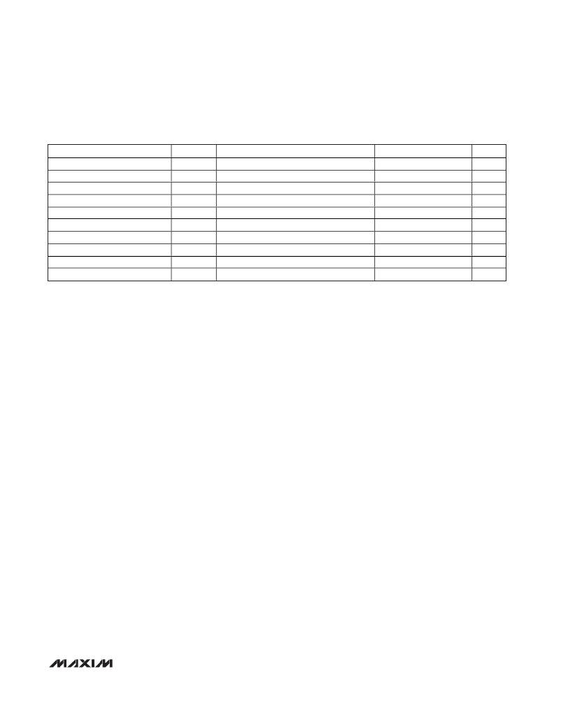
�3.5-� and� 4.5-Digit,� Single-Chip� ADCs�
�with� LCD� Drivers�
�TIMING� CHARACTERISTICS� (Notes� 10,� 11� and� Figure� 13)�
�(V� AVDD� =� V� DVDD� =� 2.7V� to� 5.25V,� V� GND� =� 0V,� T� A� =� T� MIN� to� T� MAX� ,� unless� otherwise� noted.)�
�PARAMETER�
�SCLK� Operating� Frequency�
�SYMBOL�
�f� SCLK�
�CONDITIONS�
�MIN�
�0�
�TYP�
�MAX�
�4.2�
�UNITS�
�MHz�
�SCLK� Pulse-Width� High�
�SCLK� Pulse-Width� Low�
�DIN� to� SCLK� Setup�
�DIN� to� SCLK� Hold�
�CS� Fall� to� SCLK� Rise� Setup�
�SCLK� Rise� to� CS� Rise� Hold�
�t� CH�
�t� CL�
�t� DS�
�t� DH�
�t� CSS�
�t� CSH�
�100�
�100�
�50�
�0�
�50�
�0�
�ns�
�ns�
�ns�
�ns�
�ns�
�ns�
�SCLK� Fall� to� DOUT� Valid�
�CS� Rise� to� DOUT� Disable�
�CS� Fall� to� DOUT� Enable�
�t� DO�
�t� TR�
�t� DV�
�C� LOAD� =� 50pF� (Figures� 18,� 19)�
�C� LOAD� =� 50pF� (Figures� 18,� 19)�
�C� LOAD� =� 50pF� (Figures� 18,� 19)�
�120�
�120�
�120�
�ns�
�ns�
�ns�
�Note� 1:�
�Note� 2:�
�Note� 3:�
�Note� 4:�
�Note� 5:�
�Note� 6:�
�Note� 7:�
�Note� 8:�
�Note� 9:�
�Integral� nonlinearity� is� the� deviation� of� the� analog� value� at� any� code� from� its� theoretical� value� after� nulling� the� gain� error�
�and� offset� error.�
�Offset� calibrated.� See� the� OFFSET_CAL1� and� OFFSET_CAL2� sections� in� the� On-Chip� Registers� section.�
�Offset� nulled.�
�Drift� error� is� eliminated� by� recalibration� at� the� new� temperature.�
�The� input� voltage� range� for� the� analog� inputs� is� given� with� respect� to� the� voltage� on� the� negative� input� of� the� differential� pair.�
�V� AIN+� or� V� AIN-� =� -2.2V� to� +2.2V.� V� REF+� or� V� REF-� =� -2.2V� to� +2.2V.� All� input� structures� are� identical.� Production� tested� on�
�AIN+� and� REF+� only.�
�Measured� at� DC� by� changing� the� power-supply� voltage� from� 2.7V� to� 5.25V� and� measuring� the� effect� on� the� conversion�
�error� with� external� reference.� PSRR� at� 50Hz� and� 60Hz� exceeds� 120dB� with� filter� notches� at� 50Hz� and� 60Hz� (Figure� 2).�
�CLK� and� SCLK� are� idle.�
�Power-supply� currents� are� measured� with� all� digital� inputs� at� either� GND� or� DVDD� and� with� the� device� in� internal� clock� mode.�
�Note� 10:� All� input� signals� are� specified� with� t� RISE� =� t� FALL� =� 5ns� (10%� to� 90%� of� DVDD)� and� are� timed� from� a� voltage� level� of� 50%� of�
�DVDD,� unless� otherwise� noted.�
�Note� 11:� See� the� serial-interface� timing� diagrams.�
�_______________________________________________________________________________________�
�5�
�相关PDF资料 |
PDF描述 |
|---|---|
| TPSB226K010R0500 | CAP TANT 22UF 10V 10% 1210 |
| T86D336M010ESAS | CAP TANT 33UF 10V 20% 2917 |
| MAX7221ENG+ | IC DRVR DSPLY LED 8DIG 24-DIP |
| PSAA20R-033-R-CR2 | ADAPTER WALL R-SERIES 20W 3.3V |
| T86D157M6R3ESAS | CAP TANT 150UF 6.3V 20% 2917 |
相关代理商/技术参数 |
参数描述 |
|---|---|
| MAX1492CAI+ | 功能描述:模数转换器 - ADC 3.5 Digit ADC w/LCD Drivers RoHS:否 制造商:Texas Instruments 通道数量:2 结构:Sigma-Delta 转换速率:125 SPs to 8 KSPs 分辨率:24 bit 输入类型:Differential 信噪比:107 dB 接口类型:SPI 工作电源电压:1.7 V to 3.6 V, 2.7 V to 5.25 V 最大工作温度:+ 85 C 安装风格:SMD/SMT 封装 / 箱体:VQFN-32 |
| MAX1492CAI+T | 功能描述:模数转换器 - ADC 3.5 Digit ADC w/LCD Drivers RoHS:否 制造商:Texas Instruments 通道数量:2 结构:Sigma-Delta 转换速率:125 SPs to 8 KSPs 分辨率:24 bit 输入类型:Differential 信噪比:107 dB 接口类型:SPI 工作电源电压:1.7 V to 3.6 V, 2.7 V to 5.25 V 最大工作温度:+ 85 C 安装风格:SMD/SMT 封装 / 箱体:VQFN-32 |
| MAX1492CAI-T | 功能描述:模数转换器 - ADC RoHS:否 制造商:Texas Instruments 通道数量:2 结构:Sigma-Delta 转换速率:125 SPs to 8 KSPs 分辨率:24 bit 输入类型:Differential 信噪比:107 dB 接口类型:SPI 工作电源电压:1.7 V to 3.6 V, 2.7 V to 5.25 V 最大工作温度:+ 85 C 安装风格:SMD/SMT 封装 / 箱体:VQFN-32 |
| MAX1492CNI | 功能描述:模数转换器 - ADC RoHS:否 制造商:Texas Instruments 通道数量:2 结构:Sigma-Delta 转换速率:125 SPs to 8 KSPs 分辨率:24 bit 输入类型:Differential 信噪比:107 dB 接口类型:SPI 工作电源电压:1.7 V to 3.6 V, 2.7 V to 5.25 V 最大工作温度:+ 85 C 安装风格:SMD/SMT 封装 / 箱体:VQFN-32 |
| MAX1492CNI+ | 功能描述:模数转换器 - ADC 3.5 Digit ADC w/LCD Drivers RoHS:否 制造商:Texas Instruments 通道数量:2 结构:Sigma-Delta 转换速率:125 SPs to 8 KSPs 分辨率:24 bit 输入类型:Differential 信噪比:107 dB 接口类型:SPI 工作电源电压:1.7 V to 3.6 V, 2.7 V to 5.25 V 最大工作温度:+ 85 C 安装风格:SMD/SMT 封装 / 箱体:VQFN-32 |
发布紧急采购,3分钟左右您将得到回复。