- 您现在的位置:买卖IC网 > PDF目录9899 > MAX1499ECJ+T (Maxim Integrated Products)IC ADC 3 1/2DIG W/LED DVR 32TQFP PDF资料下载
参数资料
| 型号: | MAX1499ECJ+T |
| 厂商: | Maxim Integrated Products |
| 文件页数: | 12/33页 |
| 文件大小: | 0K |
| 描述: | IC ADC 3 1/2DIG W/LED DVR 32TQFP |
| 产品培训模块: | Lead (SnPb) Finish for COTS Obsolescence Mitigation Program |
| 标准包装: | 2,000 |
| 位数: | 3.5 位 |
| 采样率(每秒): | 5 |
| 数据接口: | MICROWIRE?,QSPI?,串行,SPI? |
| 转换器数目: | 1 |
| 电压电源: | 模拟和数字 |
| 工作温度: | -40°C ~ 85°C |
| 安装类型: | 表面贴装 |
| 封装/外壳: | 32-LQFP |
| 供应商设备封装: | 32-LQFP(7x7) |
| 包装: | 带卷 (TR) |
| 输入数目和类型: | 1 个差分,双极 |
第1页第2页第3页第4页第5页第6页第7页第8页第9页第10页第11页当前第12页第13页第14页第15页第16页第17页第18页第19页第20页第21页第22页第23页第24页第25页第26页第27页第28页第29页第30页第31页第32页第33页
MAX1497/MAX1499
3.5- and 4.5-Digit, Single-Chip ADCs with LED
Drivers and C Interface
2
_______________________________________________________________________________________
ABSOLUTE MAXIMUM RATINGS
Stresses beyond those listed under “Absolute Maximum Ratings” may cause permanent damage to the device. These are stress ratings only, and functional
operation of the device at these or any other conditions beyond those indicated in the operational sections of the specifications is not implied. Exposure to
absolute maximum rating conditions for extended periods may affect device reliability.
AVDD to GND (MAX1499).........................................-0.3V to +6V
DVDD to GND (MAX1499) ........................................-0.3V to +6V
AIN+, AIN- to GND (MAX1499) ...........VNEG to (AVDD to +0.3V)
REF+, REF- to GND (MAX1499) ......... VNEG to (AVDD to +0.3V)
LOWBATT to GND (MAX1499) ................-0.3V to (AVDD + 0.3V)
CLK, EOC, CS, DIN, SCLK,
DOUT to GND (MAX1499) .......................-0.3V to (DVDD + 0.3V)
VNEG to GND (MAX1499) .......................-2.6V to (AVDD + 0.3V)
LED_EN to GND (MAX1499)....................-0.3V to (DVDD + 0.3V)
ISET to GND (MAX1499)..........................-0.3V to (AVDD + 0.3V)
VDD to GND (MAX1497) ...........................................-0.3V to +6V
AIN+, AIN- to GND (MAX1497)..............VNEG to (VDD to +0.3V)
REF+, REF- to GND (MAX1497) ........... VNEG to (VDD to +0.3V)
CLK, EOC, CS, DIN, SCLK,
DOUT to GND (MAX1497)..........................-0.3V to (VDD + 0.3V)
VNEG to GND (MAX1497)..........................-2.6V to (VDD + 0.3V)
ISET to GND (MAX1497) ............................-0.3V to (VDD + 0.3V)
VLED to GLED ..........................................................-0.3V to +6V
GLED to GND ........................................................-0.3V to +0.3V
SEG_ to GLED..........................................-0.3V to (VLED + 0.3V)
DIG_ to GLED ..........................................-0.3V to (VLED + 0.3V)
DIG_ Sink Current .............................................................300mA
DIG_ Source Current...........................................................50mA
SEG_ Sink Current ..............................................................50mA
SEG_ Source Current..........................................................50mA
Maximum Current Input into Any Other Pin ........................50mA
Continuous Power Dissipation (TA = +70°C)
32-Pin TQFP (derate 20.7mW/°C above +70°C).....1652.9mW
28-Pin SSOP (derate 9.5mW/°C above +70°C) ...........762mW
28-Pin PDIP (derate 14.3mW/°C above +70°C)......1142.9mW
Operating Temperature Range ...........................-40°C to +85°C
Junction Temperature ......................................................+150°C
Storage Temperature Range .............................-60°C to +150°C
Lead Temperature (soldering, 10s) .................................+300°C
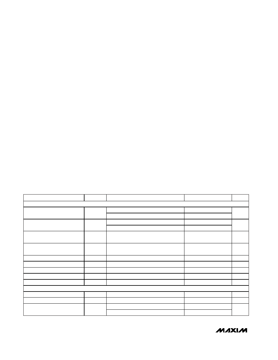
ELECTRICAL CHARACTERISTICS
(AVDD = DVDD = VDD = +2.7V to +5.25V, GND = 0, GLED = 0, VLED = +2.7V to +5.25V, VREF+ - VREF- = 2.048V (external reference)
CREF+ = CREF- = 0.1F, CVNEG = 0.1F. Internal clock mode, unless otherwise noted. All specifications are at TA = TMIN to TMAX.
Typical values are at TA = +25°C, unless otherwise noted.)
PARAMETER
SYMBOL
CONDITIONS
MIN
TYP
MAX
UNITS
DC ACCURACY
MAX1499
-19,999
+19,999
Noise-Free Resolution
MAX1497
-1999
+1999
Count
2.000V range
±1
Integral Nonlinearity (Note 1)
INL
200mV range
±1
Count
Range Change Ratio
(VAIN+ - VAIN- = 0.100V) on 200mV range
(VAIN+ - VAIN- = 0.100V) on 2.0V range
10:1
Ratio
Rollover Error
VAIN+ - VAIN- = full scale
VAIN- - VAIN+ = full scale
±1
Count
Output Noise
10
VP-P
Offset Error (Zero Input Reading)
Offset
VIN = 0 (Note 2)
-0
0
Reading
Gain Error
(Note 3)
-0.5
+0.5
%FSR
Offset Drift (Zero Reading Drift)
VIN = 0 (Note 4)
0.1
V/°C
Gain Drift
±1
ppm/°C
INPUT CONVERSION RATE
External-Clock Frequency
4.9152
MHz
External-Clock Duty Cycle
40
60
%
Internal clock
5
Conversion Rate
External clock, fCLK = 4.9152MHz
5
Hz
相关PDF资料 |
PDF描述 |
|---|---|
| MS27472E18F28S | CONN RCPT 28POS WALL MT W/SCKT |
| ISL32272EFBZ | IC XMITTER ESD RS422 LP 16-SOIC |
| ISL32179EIRZ | IC XMITTER ESD RS422 LP 24-QFN |
| ISL32174EIVZ | IC XMITTER ESD RS422 LP 16-TSSOP |
| MX7576KCWN+ | IC ADC 8BIT MPU COMP 18-SOIC |
相关代理商/技术参数 |
参数描述 |
|---|---|
| MAX1499EVC16 | 功能描述:模数转换器 - ADC 3.5- and 4.5-Digit Single-Chip ADCs with LED Drivers and uC Interface RoHS:否 制造商:Texas Instruments 通道数量:2 结构:Sigma-Delta 转换速率:125 SPs to 8 KSPs 分辨率:24 bit 输入类型:Differential 信噪比:107 dB 接口类型:SPI 工作电源电压:1.7 V to 3.6 V, 2.7 V to 5.25 V 最大工作温度:+ 85 C 安装风格:SMD/SMT 封装 / 箱体:VQFN-32 |
| MAX1499EVKIT | 功能描述:数据转换 IC 开发工具 Evaluation Kit/Evaluation System for the MAX1499 RoHS:否 制造商:Texas Instruments 产品:Demonstration Kits 类型:ADC 工具用于评估:ADS130E08 接口类型:SPI 工作电源电压:- 6 V to + 6 V |
| MAX149ACAP | 功能描述:模数转换器 - ADC Integrated Circuits (ICs) RoHS:否 制造商:Texas Instruments 通道数量:2 结构:Sigma-Delta 转换速率:125 SPs to 8 KSPs 分辨率:24 bit 输入类型:Differential 信噪比:107 dB 接口类型:SPI 工作电源电压:1.7 V to 3.6 V, 2.7 V to 5.25 V 最大工作温度:+ 85 C 安装风格:SMD/SMT 封装 / 箱体:VQFN-32 |
| MAX149ACAP+ | 功能描述:模数转换器 - ADC 10-Bit 8Ch 133ksps 5.25V Precision ADC RoHS:否 制造商:Texas Instruments 通道数量:2 结构:Sigma-Delta 转换速率:125 SPs to 8 KSPs 分辨率:24 bit 输入类型:Differential 信噪比:107 dB 接口类型:SPI 工作电源电压:1.7 V to 3.6 V, 2.7 V to 5.25 V 最大工作温度:+ 85 C 安装风格:SMD/SMT 封装 / 箱体:VQFN-32 |
| MAX149ACAP+T | 功能描述:模数转换器 - ADC 10-Bit 8Ch 133ksps 5.25V Precision ADC RoHS:否 制造商:Texas Instruments 通道数量:2 结构:Sigma-Delta 转换速率:125 SPs to 8 KSPs 分辨率:24 bit 输入类型:Differential 信噪比:107 dB 接口类型:SPI 工作电源电压:1.7 V to 3.6 V, 2.7 V to 5.25 V 最大工作温度:+ 85 C 安装风格:SMD/SMT 封装 / 箱体:VQFN-32 |
发布紧急采购,3分钟左右您将得到回复。