- 您现在的位置:买卖IC网 > PDF目录9928 > MAX152EWP+T (Maxim Integrated Products)IC ADC 8BIT 1UA PWR-DWN 20-SOIC PDF资料下载
参数资料
| 型号: | MAX152EWP+T |
| 厂商: | Maxim Integrated Products |
| 文件页数: | 11/12页 |
| 文件大小: | 0K |
| 描述: | IC ADC 8BIT 1UA PWR-DWN 20-SOIC |
| 产品培训模块: | Lead (SnPb) Finish for COTS Obsolescence Mitigation Program |
| 标准包装: | 1,000 |
| 位数: | 8 |
| 采样率(每秒): | 400k |
| 数据接口: | 并联 |
| 转换器数目: | 3 |
| 功率耗散(最大): | 800mW |
| 电压电源: | 双 ± |
| 工作温度: | -40°C ~ 85°C |
| 安装类型: | 表面贴装 |
| 封装/外壳: | 20-SOIC(0.295",7.50mm 宽) |
| 供应商设备封装: | 20-SOIC W |
| 包装: | 带卷 (TR) |
| 输入数目和类型: | 1 个单端,单极;1 个单端,双极 |
MAX152
A minimum acquisition time (tP) is required from INT
going low to the start of another conversion (
WR going
low).
Options for reading data from the converter include the
following:
Using Internal Delay
The P waits for the
INT output to go low before read-
ing the data (Figure 4).
INT goes low after the rising
edge of
WR, indicating that the conversion is complete
and the result is available in the output latch. With
CS
low, data outputs D0-D7 can be accessed by pulling
RD low. INT is then reset by the rising edge of CS or
RD.
Fastest Conversion: Reading Before Delay
An external method of controlling the conversion time is
shown in Figure 5. The internally generated delay
tINTL varies slightly with temperature and supply volt-
age, and can be overridden with
RD to achieve the
fastest conversion time.
RD is brought low after the ris-
ing edge of
WR, but before INT goes low. This com-
pletes the conversion and enables the output buffers
(D0-D7) that contain the conversion result.
INT also
goes low after the falling edge of
RD and is reset on the
rising edge of
RD or CS. The total conversion time is
therefore: tCWR = tWR (600ns) + tRD (800ns) + tACC1
(400ns) = 1800ns.
Stand-Alone Operation
Besides the two standard WR-RD mode options, stand-
alone operation can be achieved by connecting
CS
and
RD low (Figure 6). A conversion is initiated by
pulling
WR low. Output data can be read by either
edge of the next
WR pulse.
+3V, 8-Bit ADC with 1A Power-Down
8
_______________________________________________________________________________________
tP
tINTL
WR
INT
NEW DATA
tWR
tIHWR
tID
OLD DATA
D0-D7
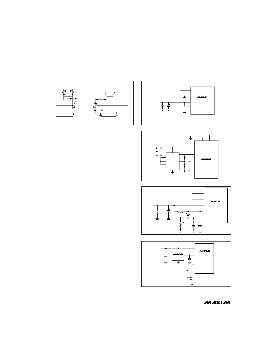
Figure 6. Stand-Alone Mode Timing (
CS = RD = 0) (MODE = 1)
VREF-
MAX152
VDD
0.1F
VIN
VREF+
VIN+
VIN-
GND
+3V
1
10
20
12
11
4.7F
Figure 7a. Power Supply as Reference
+3V
0.1
F
4
VREF-
MAX152
VREF+
VIN
8
1
3
7
0.1
F
4.7
F
2
6
GND
VDD
10
1
20
12
11
+2.5V
34.8k
3.01k
LM10
VIN+
VIN-
Figure 7b. External Reference, +2.5V Full Scale
+3V
0.1F
12
VREF-
MAX152
VREF+
VIN
10
1
20
11
0.1F
4.7F
GND
VDD
0.1F
VIN-
1.2V
VIN+
*CURRENT PATH MUST STILL
EXIST FROM VIN- TO GND.
Figure 7c. Input Not Referenced to GND
+3V
PWRDN
C1
2.2F
MTD3055EL
N
MAX152
VREF-
VDD
VREF+
PWRDN
MAX872
+
Figure 7d. An N-channel MOSFET switches off the reference
load during power-down.
相关PDF资料 |
PDF描述 |
|---|---|
| V150B28M250BG3 | CONVERTER MOD DC/DC 28V 250W |
| IDT72281L15PFI | IC FIFO 32768X18 LP 15NS 64QFP |
| ICL3243CVZ | IC 3DRVR/5RCVR RS232 3V 28-TSSOP |
| V150B28M250BF2 | CONVERTER MOD DC/DC 28V 250W |
| VI-24H-CU-B1 | CONVERTER MOD DC/DC 52V 200W |
相关代理商/技术参数 |
参数描述 |
|---|---|
| MAX152MJP | 功能描述:模数转换器 - ADC RoHS:否 制造商:Texas Instruments 通道数量:2 结构:Sigma-Delta 转换速率:125 SPs to 8 KSPs 分辨率:24 bit 输入类型:Differential 信噪比:107 dB 接口类型:SPI 工作电源电压:1.7 V to 3.6 V, 2.7 V to 5.25 V 最大工作温度:+ 85 C 安装风格:SMD/SMT 封装 / 箱体:VQFN-32 |
| MAX15300ETI+ | 功能描述:DC/DC转换器 Auto-Comp digital PoL controller RoHS:否 制造商:Murata 产品: 输出功率: 输入电压范围:3.6 V to 5.5 V 输入电压(标称): 输出端数量:1 输出电压(通道 1):3.3 V 输出电流(通道 1):600 mA 输出电压(通道 2): 输出电流(通道 2): 安装风格:SMD/SMT 封装 / 箱体尺寸: |
| MAX15300ETI+T | 功能描述:DC/DC转换器 Auto-Comp digital PoL controller RoHS:否 制造商:Murata 产品: 输出功率: 输入电压范围:3.6 V to 5.5 V 输入电压(标称): 输出端数量:1 输出电压(通道 1):3.3 V 输出电流(通道 1):600 mA 输出电压(通道 2): 输出电流(通道 2): 安装风格:SMD/SMT 封装 / 箱体尺寸: |
| MAX15301ETI+ | 功能描述:IC REG CTRLR BUCK 32TQFN RoHS:是 类别:集成电路 (IC) >> PMIC - 稳压器 - DC DC 切换控制器 系列:- 标准包装:4,000 系列:- PWM 型:电压模式 输出数:1 频率 - 最大:1.5MHz 占空比:66.7% 电源电压:4.75 V ~ 5.25 V 降压:是 升压:无 回扫:无 反相:无 倍增器:无 除法器:无 Cuk:无 隔离:无 工作温度:-40°C ~ 85°C 封装/外壳:40-VFQFN 裸露焊盘 包装:带卷 (TR) |
| MAX15301ETJ+ | 功能描述:DC/DC转换器 Auto-Comp digital PoL controller RoHS:否 制造商:Murata 产品: 输出功率: 输入电压范围:3.6 V to 5.5 V 输入电压(标称): 输出端数量:1 输出电压(通道 1):3.3 V 输出电流(通道 1):600 mA 输出电压(通道 2): 输出电流(通道 2): 安装风格:SMD/SMT 封装 / 箱体尺寸: |
发布紧急采购,3分钟左右您将得到回复。