- 您现在的位置:买卖IC网 > PDF目录383326 > MAX1579ETG (MAXIM INTEGRATED PRODUCTS INC) Complete Bias and White LED Power Supplies for Small TFT Displays PDF资料下载
参数资料
| 型号: | MAX1579ETG |
| 厂商: | MAXIM INTEGRATED PRODUCTS INC |
| 元件分类: | 显示驱动器 |
| 英文描述: | Complete Bias and White LED Power Supplies for Small TFT Displays |
| 中文描述: | LED DISPLAY DRIVER, QCC24 |
| 封装: | 4 X 4 MM, 0.80 MM HEIGHT, MO-220WGGD-2, TQFN-24 |
| 文件页数: | 2/13页 |
| 文件大小: | 221K |
| 代理商: | MAX1579ETG |
M
Complete Bias and White LED Power S upplies
for S mall T FT Displays
2
_______________________________________________________________________________________
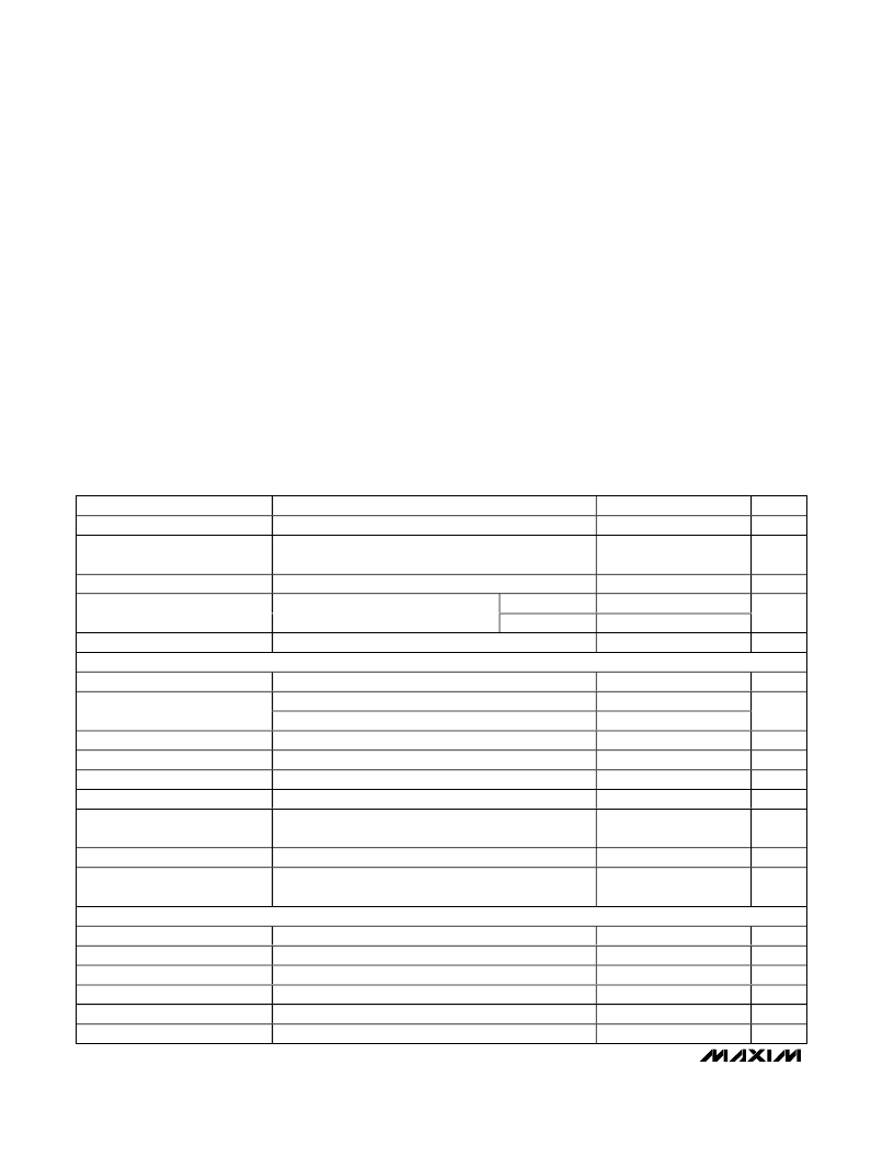
ABSOLUTE MAXIMUM RATINGS
IN, CS, C1N, C2N, MAIN, ONBIAS, V
DD
to GND.....-0.3V to +6V
CTRL to GND..................-0.3V to the lesser of +6V or (V
IN
+ 2V)
LX, OUT to GND.....................................................-0.3V to +37V
COMP to GND .............................................-0.3V to (V
IN
+ 0.3V)
CU1 to MAIN ............................................................-0.3V to +6V
CU2 to CU1..............................................................-0.3V to +6V
CU3 to CU2..............................................................-0.3V to +6V
CU3 to POS ............................................................-0.3V to +18V
CU3 to GND ...........................................................-0.3V to +18V
POS to GND ...........................................................-0.3V to +18V
CD1 to MAIN ..........................................................+0.3V to -12V
CD1 to GND .............................................................+0.3V to -6V
CD2 to CD1..............................................................+0.3V to -6V
NEG to CD2..............................................................+0.3V to -6V
ELECTRICAL CHARACTERISTICS
(Circuit of Figure 3, V
IN
= 3V, CTRL = ONBIAS = IN, T
A
= -40
°
C to +85
°
C, typical values are at T
A
= +25
°
C, unless otherwise noted. Note 1)
PARAMETER
CONDITIONS
IN Operating Supply Range
Stresses beyond those listed under “Absolute Maximum Ratings” may cause permanent damage to the device. These are stress ratings only, and functional
operation of the device at these or any other conditions beyond those indicated in the operational sections of the specifications is not implied. Exposure to
absolute maximum rating conditions for extended periods may affect device reliability.
NEG, CD2 to GND..................................................+0.3V to -12V
C1P, C2P to GND ...........................................-0.3V to (V
IN
+ 6V)
PMP, PMPB to GND................................-0.3V to (V
MAIN
+ 0.3V)
GND to PGND .......................................................-0.3V to +0.3V
I
LX
...................................................................................1.0A
RMS
Continuous Power Dissipation (T
A
= +70
°
C)
24-Pin 4mm x 4mm Thin QFN
(derate 20.8mW/
°
C above +70
°
C) .............................1667mW
Short-Circuit Duration (MAIN, POS, NEG)..................Continuous
Operating Temperature Range ...........................-40
°
C to +85
°
C
J unction Temperature......................................................+150
°
C
Storage Temperature Range.............................-65
°
C to +150°C
Lead Temperature (soldering, 10s) ................................ +300
°
C
MIN
2.7
TYP
MAX
5.5
UNITS
V
IN Undervoltage-Lockout (UVLO)
Threshold
Rising edge, 30mV hysteresis
2.1
2.35
2.6
V
IN Quiescent Current
Switching
3
5
1
mA
T
A
= +25°C
T
A
= +85°C
0.4
1
+160
IN Shutdown Current
V
CTRL
= V
ONBIAS
= 0V
μA
Thermal Shutdown
MAIN CHARGE PUMP WITH LINEAR REGULATOR
Main Pump Efficiency
Rising temperature, 20°C hysteresis (typ)
°C
I
LOAD
= 25mA, V
IN
= 3.9V
V
IN
≥
3.8V in 1.5x mode
V
IN
≥
3.0V in 2.0x mode
83
9
7.5
250
5.5
3.85
3.9
%
20
20
300
5.7
3.95
4.0
V
DD
Charge-Pump Open-Loop
Output Impedance
Operating Frequency
V
DD
Output Voltage
V
IN
Fal ng S w chover to 2.0x M od e
V
IN
Ri si ng S w chover to 1.5x M od e
Quiescent Current
(Charge Pumps Only)
200
5.2
3.75
3.8
kHz
V
V
V
Charge-pump pause threshold
V
CTRL
= 0V, ONBIAS = IN
0.87
1.30
mA
V
MAIN
Regulation Voltage
Discharge Switch Resistance
at V
MAIN
POS, NEG CHARGE PUMPS
Operating Frequency
Duty Cycle
POS Pump Efficiency
POS Output Voltage
P OS D schar g e S w ch Resi stance
NEG Pump Efficiency
0.1mA < I
LOAD
< 25mA
4.9
5.0
5.1
V
V
ONBIAS
= 0V
1
3
k
12.0
15.6
50
97
14.7
3
97
19.5
kHz
%
%
V
k
%
I
LOAD
= 100μA
I
LOAD
= 0 to 100μA
V
ONBIAS
= 0V
I
LOAD
= -100μA
13.9
15.3
6
相关PDF资料 |
PDF描述 |
|---|---|
| MAX1584 | 5-Channel Slim DSC Power Supplies |
| MAX1585 | 5-Channel Slim DSC Power Supplies |
| MAX1584-MAX1585 | 5-Channel Slim DSC Power Supplies |
| MAX1584ETJ | 5-Channel Slim DSC Power Supplies |
| MAX1585ETJ | 5-Channel Slim DSC Power Supplies |
相关代理商/技术参数 |
参数描述 |
|---|---|
| MAX1579ETG+ | 功能描述:LED照明驱动器 Cmplete Bias & White LED Power Supply RoHS:否 制造商:STMicroelectronics 输入电压:11.5 V to 23 V 工作频率: 最大电源电流:1.7 mA 输出电流: 最大工作温度: 安装风格:SMD/SMT 封装 / 箱体:SO-16N |
| MAX1579ETG+T | 功能描述:LED照明驱动器 Cmplete Bias & White LED Power Supply RoHS:否 制造商:STMicroelectronics 输入电压:11.5 V to 23 V 工作频率: 最大电源电流:1.7 mA 输出电流: 最大工作温度: 安装风格:SMD/SMT 封装 / 箱体:SO-16N |
| MAX1579ETG-T | 功能描述:LED照明驱动器 RoHS:否 制造商:STMicroelectronics 输入电压:11.5 V to 23 V 工作频率: 最大电源电流:1.7 mA 输出电流: 最大工作温度: 安装风格:SMD/SMT 封装 / 箱体:SO-16N |
| MAX1579EVKIT | 功能描述:LED 照明开发工具 Evaluation Kit for the MAX1579 RoHS:否 制造商:Fairchild Semiconductor 产品:Evaluation Kits 用于:FL7732 核心: 电源电压:120V 系列: 封装: |
| MAX157ACPA | 功能描述:模数转换器 - ADC RoHS:否 制造商:Texas Instruments 通道数量:2 结构:Sigma-Delta 转换速率:125 SPs to 8 KSPs 分辨率:24 bit 输入类型:Differential 信噪比:107 dB 接口类型:SPI 工作电源电压:1.7 V to 3.6 V, 2.7 V to 5.25 V 最大工作温度:+ 85 C 安装风格:SMD/SMT 封装 / 箱体:VQFN-32 |
发布紧急采购,3分钟左右您将得到回复。