- 您现在的位置:买卖IC网 > PDF目录9915 > MAX157ACPA+ (Maxim Integrated Products)IC ADC 10BIT 108KSPS 2CH 8-DIP PDF资料下载
参数资料
| 型号: | MAX157ACPA+ |
| 厂商: | Maxim Integrated Products |
| 文件页数: | 3/16页 |
| 文件大小: | 0K |
| 描述: | IC ADC 10BIT 108KSPS 2CH 8-DIP |
| 产品培训模块: | Lead (SnPb) Finish for COTS Obsolescence Mitigation Program |
| 标准包装: | 50 |
| 位数: | 10 |
| 采样率(每秒): | 108k |
| 数据接口: | MICROWIRE?,QSPI?,串行,SPI? |
| 转换器数目: | 1 |
| 功率耗散(最大): | 727mW |
| 电压电源: | 单电源 |
| 工作温度: | 0°C ~ 70°C |
| 安装类型: | 通孔 |
| 封装/外壳: | 8-DIP(0.300",7.62mm) |
| 供应商设备封装: | 8-PDIP |
| 包装: | 管件 |
| 输入数目和类型: | 2 个单端,单极 |
etc. Therefore, SNR is computed by taking the ratio of
the RMS signal to the RMS noise (which includes all
spectral components minus the fundamental), the first
five harmonics, and the DC offset.
Signal-to-Noise Plus Distortion (SINAD)
Signal-to-noise plus distortion is the ratio of the funda-
mental input frequency’s RMS amplitude to RMS equiv-
alent of all other ADC output signals:
Effective Number of Bits (ENOB)
ENOB indicates the global accuracy of an ADC at a
specific input frequency and sampling rate. An ideal
ADC’s error consists of quantization noise only. With an
input range equal to the full-scale range of the ADC,
calculate the effective number of bits as follows:
ENOB = (SINAD - 1.76) / 6.02
Total Harmonic Distortion (THD)
THD is the ratio of the RMS sum of the first five harmon-
ics of the input signal to the fundamental itself. This is
expressed as:
where V1 is the fundamental amplitude and V2 through
V5 are the amplitudes of the 2nd through 5th-order har-
monics.
Spurious-Free Dynamic Range (SFDR)
SFDR is the ratio of RMS amplitude of the fundamental
(maximum signal component) to the RMS value of the
next largest spurious component, excluding DC offset.
Connection to Standard Interfaces
The MAX157/MAX159 interface is fully compatible with
SPI/QSPI and MICROWIRE standard serial interfaces.
If a serial interface is available, establish the CPU’s seri-
al interface as master so that the CPU generates the
serial clock for the MAX157/MAX159. Select a clock fre-
quency from 100kHz to 2.17MHz (external clock mode).
1) Use a general-purpose I/O line on the CPU to pull
CS/SHDN low while SCLK is low.
2) Wait for the minimum wake-up time (tWAKE) speci-
fied before activating SCLK.
3) Activate SCLK for a minimum of 16 clock cycles. The
first falling clock edge will generate a serial data-
stream of three leading ones, followed by the chan-
nel identification, the MSB of the digitized input
signal, and two sub-bits. DOUT transitions on
SCLK’s falling edge and is available in MSB-first for-
mat. Observe the SCLK to DOUT valid timing char-
acteristic. Data should be clocked into the P on
SCLK’s rising edge.
4) Pull CS/SHDN high at or after the 16th falling clock
edge. If CS/SHDN remains low, trailing zeros will be
clocked out after the sub-bits.
5) With CS/SHDN high, wait at least 60ns (tCS), before
starting a new conversion by pulling CS/SHDN low.
A conversion can be aborted by pulling CS/SHDN
high before the conversion ends; wait at least 60ns
before starting a new conversion.
Data can be output either in two 8-bit sequences or
continuously. The bytes will contain the result of the
conversion padded with three leading ones, the chan-
nel identification before the MSB, and two trailing sub-
bits. If the serial clock hasn’t been idled after the last
sub-bit (S0) and CS/SHDN is kept low, DOUT sends
trailing zeros.
SPI and MICROWIRE Interface
When using SPI (Figure 8a) or MICROWIRE (Figure 8b)
interfaces, set CPOL = 0 and CPHA = 0. Conversion
begins with a falling edge on CS/SHDN (Figure 8c). Two
consecutive 8-bit readings are necessary to obtain the
entire 10-bit result from the ADC. DOUT data transitions
on the serial clock’s falling edge and is clocked into the
P on SCLK’s rising edge. The first 8-bit data stream
contains three leading ones, followed by channel identi-
fication and the first four data bits starting with the MSB.
The second 8-bit data stream contains the remaining
bits, D5 through D0, and the sub-bits S1 and S0.
THD = 20
log
V
+ V
V
22
32
42
52
12
()
SINAD(dB) = 20
log
Signal
(Noise + Distortion)
RMS
MAX157/MAX159
+2.7V, Low-Power, 2-Channel,
108ksps, Serial 10-Bit ADCs in 8-Pin MAX
______________________________________________________________________________________
11
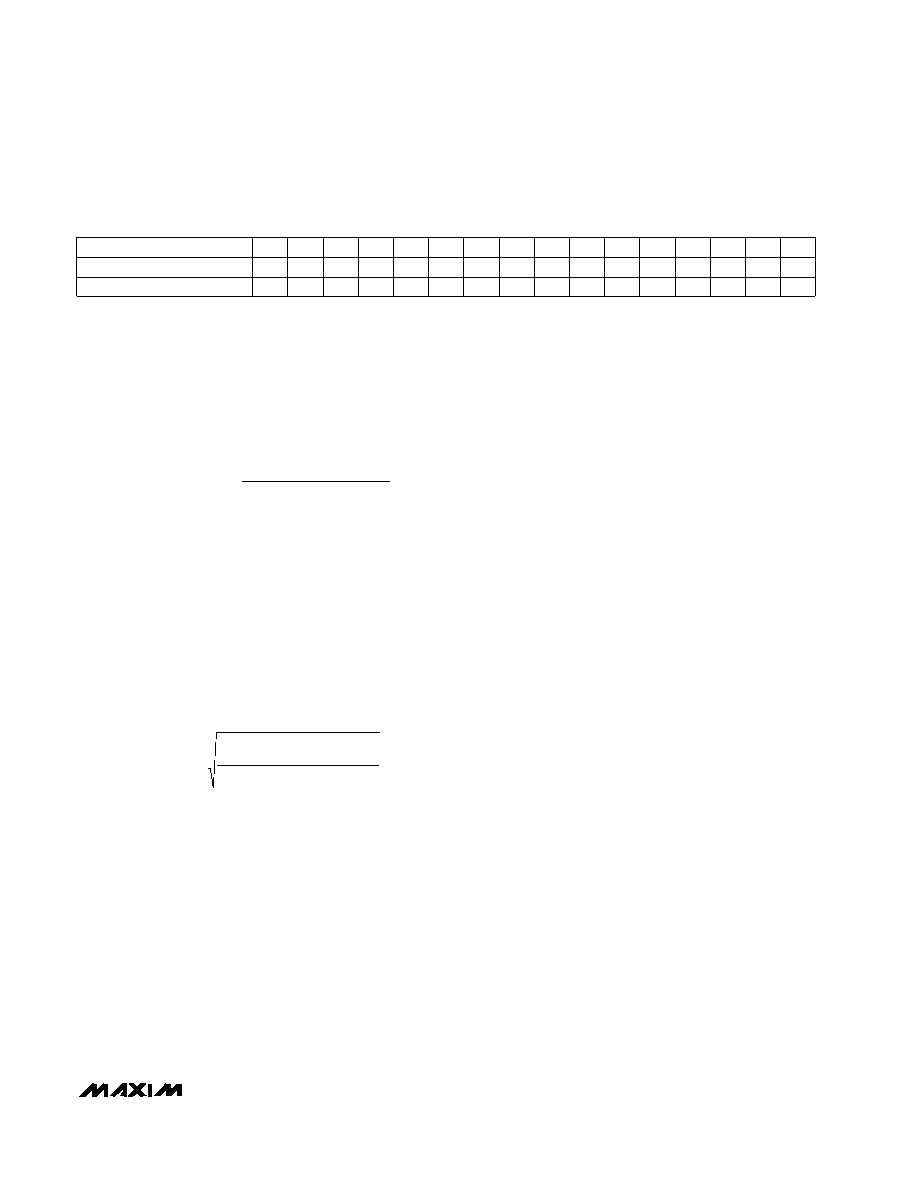
Table 1. Serial Output Data Stream for Internal and External Clock Mode
D0
D1
D2
D3
D4
D5
D6
D7
D8
D9
CHID
1
EOC
DOUT (Internal Clock)
14
13
12
11
10
9
8
7
6
5
4
3
2
1
SCLK CYCLE
D0
D1
D2
D3
D4
D5
D6
D7
D8
D9
CHID
1
DOUT (External Clock)
S0
S1
S0
S1
16
15
相关PDF资料 |
PDF描述 |
|---|---|
| VI-BW1-MW-F2 | CONVERTER MOD DC/DC 12V 100W |
| MAX159ACUA+ | IC ADC 10BIT 108KSPS 8-UMAX |
| HIN211EIBZ | IC 4DRVR/5RCVR RS232 5V 28-SOIC |
| VI-2WV-MX-F3 | CONVERTER MOD DC/DC 5.8V 75W |
| IDT723652L15PF | IC FIFO BI SYNC 4096X36 120QFP |
相关代理商/技术参数 |
参数描述 |
|---|---|
| MAX157ACPA+ | 功能描述:模数转换器 - ADC 10-Bit 2Ch 108ksps 5.25V Precision ADC RoHS:否 制造商:Texas Instruments 通道数量:2 结构:Sigma-Delta 转换速率:125 SPs to 8 KSPs 分辨率:24 bit 输入类型:Differential 信噪比:107 dB 接口类型:SPI 工作电源电压:1.7 V to 3.6 V, 2.7 V to 5.25 V 最大工作温度:+ 85 C 安装风格:SMD/SMT 封装 / 箱体:VQFN-32 |
| MAX157ACUA | 功能描述:模数转换器 - ADC RoHS:否 制造商:Texas Instruments 通道数量:2 结构:Sigma-Delta 转换速率:125 SPs to 8 KSPs 分辨率:24 bit 输入类型:Differential 信噪比:107 dB 接口类型:SPI 工作电源电压:1.7 V to 3.6 V, 2.7 V to 5.25 V 最大工作温度:+ 85 C 安装风格:SMD/SMT 封装 / 箱体:VQFN-32 |
| MAX157ACUA+ | 功能描述:模数转换器 - ADC 10-Bit 2Ch 108ksps 5.25V Precision ADC RoHS:否 制造商:Texas Instruments 通道数量:2 结构:Sigma-Delta 转换速率:125 SPs to 8 KSPs 分辨率:24 bit 输入类型:Differential 信噪比:107 dB 接口类型:SPI 工作电源电压:1.7 V to 3.6 V, 2.7 V to 5.25 V 最大工作温度:+ 85 C 安装风格:SMD/SMT 封装 / 箱体:VQFN-32 |
| MAX157ACUA+T | 功能描述:模数转换器 - ADC 10-Bit 2Ch 108ksps 5.25V Precision ADC RoHS:否 制造商:Texas Instruments 通道数量:2 结构:Sigma-Delta 转换速率:125 SPs to 8 KSPs 分辨率:24 bit 输入类型:Differential 信噪比:107 dB 接口类型:SPI 工作电源电压:1.7 V to 3.6 V, 2.7 V to 5.25 V 最大工作温度:+ 85 C 安装风格:SMD/SMT 封装 / 箱体:VQFN-32 |
| MAX157ACUA-T | 功能描述:模数转换器 - ADC RoHS:否 制造商:Texas Instruments 通道数量:2 结构:Sigma-Delta 转换速率:125 SPs to 8 KSPs 分辨率:24 bit 输入类型:Differential 信噪比:107 dB 接口类型:SPI 工作电源电压:1.7 V to 3.6 V, 2.7 V to 5.25 V 最大工作温度:+ 85 C 安装风格:SMD/SMT 封装 / 箱体:VQFN-32 |
发布紧急采购,3分钟左右您将得到回复。