- 您现在的位置:买卖IC网 > PDF目录14507 > MAX1606EUA+ (Maxim Integrated Products)IC REG BOOST ADJ 0.5A 8UMAX PDF资料下载
参数资料
| 型号: | MAX1606EUA+ |
| 厂商: | Maxim Integrated Products |
| 文件页数: | 8/10页 |
| 文件大小: | 0K |
| 描述: | IC REG BOOST ADJ 0.5A 8UMAX |
| 产品培训模块: | Lead (SnPb) Finish for COTS Obsolescence Mitigation Program |
| 标准包装: | 50 |
| 类型: | 升压(升压) |
| 输出类型: | 可调式 |
| 输出数: | 1 |
| 输出电压: | 0.8 V ~ 28 V |
| 输入电压: | 2.4 V ~ 5.5 V |
| 频率 - 开关: | 500kHz |
| 电流 - 输出: | 500mA |
| 同步整流器: | 无 |
| 工作温度: | -40°C ~ 85°C |
| 安装类型: | 表面贴装 |
| 封装/外壳: | 8-TSSOP,8-MSOP(0.118",3.00mm 宽) |
| 包装: | 管件 |
| 供应商设备封装: | 8-uMAX |
| 产品目录页面: | 1410 (CN2011-ZH PDF) |
�� �
�
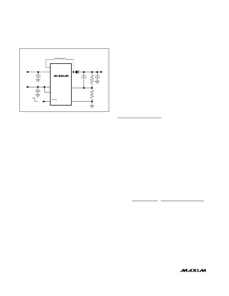
�28V� Internal� Switch� LCD� Bias� Supply�
�with� True� Shutdown�
�output� rectifier,� holding� the� output� voltage� to� one� diode�
�L1�
�10� μ� H�
�drop� below� V� IN� when� the� converter� is� shutdown� and�
�allowing� the� output� to� draw� power� from� the� input.� The�
�MAX1606� features� true� shutdown,� which� uses� an� internal�
�V� BATT� =� 0.8V� TO� 5.5V�
�C2�
�10� μ� F�
�V� CC� =� 2.4V� TO� 5.5V�
�C1�
�1� μ� F�
�ON�
�SW�
�BATT�
�V� CC�
�LIM�
�MAX1606�
�LX�
�FB�
�D1�
�C� FF�
�10pF�
�R1�
�1M� ?�
�R2�
�75k�
�V� OUT� =� 18V�
�C� OUT�
�1� μ� F�
�P-channel� MOSFET� to� disconnect� the� output� from� the�
�input� when� the� MAX1606� is� shutdown.� This� eliminates�
�power� drawn� from� the� input� during� shutdown.�
�Separate/Same� Power� for� V� BATT� and� V� CC�
�Separate� voltage� sources� can� supply� the� inductor�
�(V� BATT� )� and� the� IC� (V� CC� ).� Since� the� chip� bias� is� provid-�
�ed� by� a� logic� supply� (2.4V� to� 5.5V),� this� allows� the� out-�
�put� power� to� be� sourced� directly� from� low-voltage�
�OFF�
�SHDN�
�GND�
�batteries� (0.8V� to� 5.5V).� Conversely,� V� BATT� and� V� CC�
�can� also� be� supplied� from� one� supply� if� it� remains� with-�
�in� V� CC� ’s� operating� limits� (2.4V� to� 5.5V).�
�Figure� 3.� Typical� Application� Circuit�
�Setting� the� Output� Voltage� (FB)�
�Adjust� the� output� voltage� by� connecting� a� voltage-�
�divider� from� the� output� (V� OUT� )� to� FB� (Figure� 3).� Select�
�R2� between� 10k� ?� and� 200k� ?� .� Calculate� R1� with� the� fol-�
�lowing� equation:�
�R1� =� R2� [(V� OUT� /� V� FB� )� –� 1]�
�where� V� FB� =� 1.25V� and� V� OUT� may� range� from� V� BATT� to�
�28V.� The� input� bias� current� of� FB� has� a� maximum� value�
�of� 100nA,� which� allows� large-value� resistors� to� be� used.�
�For� less� than� 1%� error,� the� current� through� R2� should�
�be� greater� than� 100� times� the� feedback� input� bias� cur-�
�rent� (I� FB� ).�
�Current-Limit� Select� Pin� (LIM)�
�The� MAX1606� allows� a� selectable� inductor� current� limit�
�of� 125mA,� 250mA,� or� 500mA� (Figure� 2).� This� allows�
�Design� Procedure�
�Inductor� Selection�
�Smaller� inductance� values� typically� offer� smaller� physi-�
�cal� size� for� a� given� series� resistance� or� saturation� cur-�
�rent.� Circuits� using� larger� inductance� values� may� start�
�up� at� lower� input� voltages� and� exhibit� less� ripple,� but�
�also� provide� reduced� output� power.� This� occurs� when�
�the� inductance� is� sufficiently� large� to� prevent� the� maxi-�
�mum� current� limit� from� being� reached� before� the� maxi-�
�mum� on-time� expires.� The� inductor’s� saturation� current�
�rating� should� be� greater� than� the� peak� switching� cur-�
�rent.� However,� it� is� generally� acceptable� to� bias� the�
�inductor� into� saturation� by� as� much� as� 20%,� although�
�this� will� slightly� reduce� efficiency.�
�Picking� the� Current� Limit�
�The� peak� LX� current� limit� (I� LX(MAX)� )� required� for� the�
�application� may� be� calculated� from� the� following� equa-�
�tion:�
�(� V� OUT� BATT� (� MIN� )� )� � t� OFF� (� MIN� )�
�flexibility� in� designing� for� higher� current� applications� or�
�for� smaller,� compact� designs.� The� lower� current� limit�
�allows� the� use� of� a� physically� smaller� inductor� in� space-�
�I� LX� (� MAX� )� ≥�
�V� OUT� � I� OUT� (� MAX� )�
�V� BATT� (� MIN� )�
�+�
�?� V�
�2� � L�
�sensitive,� low-power� applications.� Connect� LIM� to� V� CC�
�for� 500mA,� leave� floating� for� 250mA,� or� connect� to�
�GND� for� 125mA.�
�Shutdown� (� SHDN� )�
�Pull� SHDN� low� to� enter� shutdown.� During� shutdown� the�
�supply� current� drops� to� 0.1μA,� the� output� is� discon-�
�nected� from� the� input,� and� LX� enters� a� high-impedance�
�state.� The� capacitance� and� load� at� the� output� deter-�
�mine� the� rate� at� which� V� OUT� decays.� SHDN� can� be�
�pulled� as� high� as� 6V,� regardless� of� the� input� and� output�
�voltages.�
�With� the� typical� step-up� converter� circuit,� the� output�
�remains� connected� to� the� input� through� the� inductor� and�
�where� t� OFF(MIN)� =� 0.8μs,� and� V� BATT(MIN)� is� the� mini-�
�mum� voltage� used� to� supply� the� inductor.� The� set� cur-�
�rent� limit� must� be� greater� than� this� calculated� value.�
�Select� the� appropriate� current� limit� by� connecting� LIM�
�to� V� CC� ,� GND,� or� leaving� it� unconnected� (see� Current-�
�Limit� Select� Pin� and� Figure� 2).�
�Diode� Selection�
�The� high� switching� frequency� of� 500kHz� requires� a� high-�
�speed� rectifier.� Schottky� diodes,� such� as� the� Motorola�
�MBRS0530� or� the� Nihon� EP05Q03L,� are� recommended.�
�To� maintain� high� efficiency,� the� average� current� rating� of�
�the� Schottky� diode� should� be� greater� than� the� peak�
�8�
�_______________________________________________________________________________________�
�相关PDF资料 |
PDF描述 |
|---|---|
| ECC43DCMI-S288 | CONN EDGECARD 86POS .100 EXTEND |
| VI-B11-EX-F2 | CONVERTER MOD DC/DC 12V 75W |
| MAX5035CUSA+ | IC REG BUCK 12V 1A 8SOIC |
| 2223-H-RC | INDUCTOR TORD HI AMP 820UH HORZ |
| MAX5035BUSA+ | IC REG BUCK 5V 1A 8SOIC |
相关代理商/技术参数 |
参数描述 |
|---|---|
| MAX1606EUA.C71076 | 制造商:Maxim Integrated Products 功能描述: |
| MAX1606EUA+ | 功能描述:LCD 驱动器 28V Int Switch LCD Bias Supply RoHS:否 制造商:Maxim Integrated 数位数量:4.5 片段数量:30 最大时钟频率:19 KHz 工作电源电压:3 V to 3.6 V 最大工作温度:+ 85 C 最小工作温度:- 20 C 封装 / 箱体:PDIP-40 封装:Tube |
| MAX1606EUA+T | 功能描述:LCD 驱动器 28V Int Switch LCD Bias Supply RoHS:否 制造商:Maxim Integrated 数位数量:4.5 片段数量:30 最大时钟频率:19 KHz 工作电源电压:3 V to 3.6 V 最大工作温度:+ 85 C 最小工作温度:- 20 C 封装 / 箱体:PDIP-40 封装:Tube |
| MAX1606EUA-T | 功能描述:LCD 驱动器 28V Int Switch LCD Bias Supply RoHS:否 制造商:Maxim Integrated 数位数量:4.5 片段数量:30 最大时钟频率:19 KHz 工作电源电压:3 V to 3.6 V 最大工作温度:+ 85 C 最小工作温度:- 20 C 封装 / 箱体:PDIP-40 封装:Tube |
| MAX1606EUA-TG069 | 制造商:Rochester Electronics LLC 功能描述: 制造商:Maxim Integrated Products 功能描述: |
发布紧急采购,3分钟左右您将得到回复。