- 您现在的位置:买卖IC网 > PDF目录1838 > MAX1626ESA-T (Maxim Integrated Products)IC REG CTRLR BUCK PWM CM 8-SOIC PDF资料下载
参数资料
| 型号: | MAX1626ESA-T |
| 厂商: | Maxim Integrated Products |
| 文件页数: | 12/16页 |
| 文件大小: | 0K |
| 描述: | IC REG CTRLR BUCK PWM CM 8-SOIC |
| 产品培训模块: | Lead (SnPb) Finish for COTS Obsolescence Mitigation Program |
| 标准包装: | 2,500 |
| PWM 型: | 电流模式 |
| 输出数: | 1 |
| 频率 - 最大: | 300kHz |
| 占空比: | 100% |
| 电源电压: | 3 V ~ 16.5 V |
| 降压: | 是 |
| 升压: | 无 |
| 回扫: | 无 |
| 反相: | 无 |
| 倍增器: | 无 |
| 除法器: | 无 |
| Cuk: | 无 |
| 隔离: | 无 |
| 工作温度: | -40°C ~ 85°C |
| 封装/外壳: | 8-SOIC(0.154",3.90mm 宽) |
| 包装: | 带卷 (TR) |
�� �
�
�5V/3.3V� or� Adjustable,� 100%� Duty-Cycle,�
�High-Efficiency,� Step-Down� DC-DC� Controllers�
�current� feedback� signal� and� causing� jitter.� 0.47μF� is�
�recommended.� Increase� the� value� as� necessary� in�
�high-power� applications.�
�Bypass� REF� with� 0.1μF.� This� capacitor� should� be�
�placed� within� 0.2� inches� (5mm)� of� the� IC,� next� to� REF,�
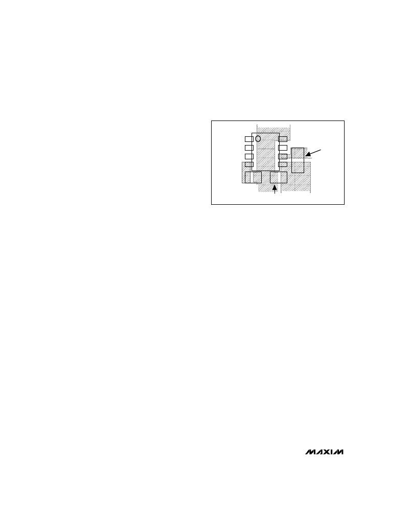
�with� a� direct� trace� to� GND� (Figure� 7).�
�Layout� Considerations�
�High-frequency� switching� regulators� are� sensitive� to� PC�
�board� layout.� Poor� layout� introduces� switching� noise� into�
�MAX1626�
�4x�
�SCALE�
�R� SENSE�
�the� current� and� voltage� feedback� signals,� resulting� in� jit-�
�ter,� instability,� or� degraded� performance.� The� current-�
�sense� resistor� must� be� placed� within� 0.2� inches� (5mm)�
�of� the� controller� IC,� directly� between� V+� and� CS.� Place�
�voltage� feedback� resistors� (MAX1627)� next� to� the� FB� pin�
�(no� more� than� 0.2")� rather� than� near� the� output.� Place�
�the� 0.47μF� input� and� 0.1μF� reference� bypass� capacitors�
�within� 0.2� inches� (5mm)� of� V+� and� REF,� and� route�
�directly� to� GND.� Figure� 7� shows� the� recommended� lay-�
�out� and� routing� for� these� components.�
�High-power� traces,� highlighted� in� the� Typical� Operating�
�Circuit� (Figure� 1),� should� be� as� short� and� as� wide� as�
�possible.� The� supply-current� loop� (formed� by� C2,� C3,�
�R� SENSE� ,� U1,� L1,� and� C1)� and� commutation-current� loop�
�(D1,� L1,� and� C1)� should� be� as� tight� as� possible� to�
�reduce� radiated� noise.� Place� the� anode� of� the� commuta-�
�tion� diode� (D1)� and� the� ground� pins� of� the� input� and�
�output� filter� capacitors� close� together,� and� route� them� to�
�a� common� “star-ground”� point.� Place� components� and�
�route� ground� paths� so� as� to� prevent� high� currents� from�
�causing� large� voltage� gradients� between� the� ground� pin�
�of� the� output� filter� capacitor,� the� controller� IC,� and� the�
�reference� bypass� capacitor.� Keep� the� extra� copper� on�
�the� component� and� solder� sides� of� the� PC� board,� rather�
�than� etching� it� away,� and� connect� it� to� ground� for� use� as�
�a� pseudo-ground� plane.� Refer� to� the� MAX1626�
�Evaluation� Kit� manual� for� a� two-layer� PC� board� example.�
�Stability� and� MAX1627� Feedback�
�Compensation�
�Use� proper� PC� board� layout� and� recommended� exter-�
�nal� components� to� ensure� stable� operation.� In� one-�
�shot,� sequenced� PFM� DC-DC� converters,� instability� is�
�manifested� as� “Motorboat� Instability.� ”� It� is� usually�
�caused� by� excessive� noise� on� the� current� or� voltage�
�feedback� signals,� ground,� or� reference,� due� to� poor� PC�
�board� design� or� external� component� selection.�
�Motorboat� instability� is� characterized� by� grouped�
�switching� pulses� with� large� gaps� and� excessive� low-�
�frequency� output� ripple.� It� is� normal� to� see� some�
�grouped� switching� pulses� during� the� transition� from�
�discontinuous� to� continuous� current� mode.� This� effect�
�is� associated� with� small� gaps� between� pulse� groups�
�C� REF�
�C� V+� BYPASS�
�Figure� 7.� Recommended� Placement� and� Routing� of� the�
�Current-Sense� Resistor,� 0.1μF� Reference,� and� 0.47μF� Input�
�Bypass� Capacitors�
�and� output� ripple� similar� to� or� less� than� that� seen� dur-�
�ing� no-load� conditions.�
�Instability� can� also� be� caused� by� excessive� stray� capaci-�
�tance� on� FB� when� using� the� MAX1627.� Compensate� for�
�this� by� adding� a� 0pF� to� 330pF� feed-forward� capacitor�
�across� the� upper� feedback� resistor� (R2� in� Figure� 5).�
�MAX1626/MAX1627� vs.�
�MAX1649/MAX1651� vs.�
�MAX649/MAX651�
�The� MAX1626/MAX1627� are� specialized,� third-genera-�
�tion� upgrades� to� the� MAX649/MAX651� step-down� con-�
�trollers.� They� feature� improved� efficiency,� a� reduced�
�current-sense� threshold� (100mV),� soft-start,� and� a�
�100%� duty� cycle� for� lowest� dropout.� The� MAX649/�
�MAX651� have� a� two-step� (210mV/110mV)� current-�
�sense� threshold.� The� MAX1649/MAX1651� are� second-�
�generation� upgrades� with� a� 96.5%� maximum� duty� cycle�
�for� improved� dropout� performance� and� a� reduced� cur-�
�rent-sense� threshold� (110mV)� for� higher� efficiency,�
�especially� at� low� input� voltages.� The� MAX1649/�
�MAX1651� are� preferable� for� special� applications� where�
�a� 100%� duty� cycle� is� undesirable,� such� as� flyback� and�
�SEPIC� circuits.�
�Since� the� MAX1626’s� pinout� is� similar� to� those� of� the�
�MAX649� and� MAX1649� family� parts,� the� MAX1626� can�
�be� substituted� (with� minor� external� component� value�
�changes)� into� fixed-output� mode� applications,� provided�
�the� PC� board� layout� is� adequate.� The� MAX1627� can�
�also� be� substituted� when� MAX649� or� MAX1649� family�
�parts� are� used� in� adjustable� mode,� but� the� feedback�
�resistor� values� must� be� changed,� since� the� MAX1627�
�has� a� lower� reference� voltage� (1.3V� vs.� 1.5V).� Reduce�
�the� current-sense� resistor� value� by� 50%� when� substitut-�
�ing� for� the� MAX649� or� MAX651.�
�12�
�______________________________________________________________________________________�
�相关PDF资料 |
PDF描述 |
|---|---|
| MAX1631EAI | IC REG CTRLR BUCK PWM CM 28-SSOP |
| MAX1634AEAI+ | IC REG CTRLR BUCK PWM CM 28-SSOP |
| MAX1636EAP+T | IC REG CTRLR BUCK PWM CM 20-SSOP |
| MAX1637EEE | IC REG CTRLR BUCK PWM CM 16-QSOP |
| MAX1638EAG+T | IC STEP-DWN CTRLR HI-SPD 24-SSOP |
相关代理商/技术参数 |
参数描述 |
|---|---|
| MAX1626EVKIT | 功能描述:DC/DC 开关控制器 3V/3.3V 100% Duty-Cycle High-Efficiency Step-Down DC-DC Controller RoHS:否 制造商:Texas Instruments 输入电压:6 V to 100 V 开关频率: 输出电压:1.215 V to 80 V 输出电流:3.5 A 输出端数量:1 最大工作温度:+ 125 C 安装风格: 封装 / 箱体:CPAK |
| MAX1626EVKIT-SO | 功能描述:DC/DC 开关控制器 Evaluation Kit for the MAX1626 MAX1627 RoHS:否 制造商:Texas Instruments 输入电压:6 V to 100 V 开关频率: 输出电压:1.215 V to 80 V 输出电流:3.5 A 输出端数量:1 最大工作温度:+ 125 C 安装风格: 封装 / 箱体:CPAK |
| MAX1627ESA | 功能描述:DC/DC 开关控制器 5/3.3V or Adjustable 100% Duty Cycle RoHS:否 制造商:Texas Instruments 输入电压:6 V to 100 V 开关频率: 输出电压:1.215 V to 80 V 输出电流:3.5 A 输出端数量:1 最大工作温度:+ 125 C 安装风格: 封装 / 箱体:CPAK |
| MAX1627ESA+ | 功能描述:DC/DC 开关控制器 5/3.3V or Adjustable 100% Duty Cycle RoHS:否 制造商:Texas Instruments 输入电压:6 V to 100 V 开关频率: 输出电压:1.215 V to 80 V 输出电流:3.5 A 输出端数量:1 最大工作温度:+ 125 C 安装风格: 封装 / 箱体:CPAK |
| MAX1627ESA+ | 制造商:Maxim Integrated Products 功能描述:CONTROLLER STEP DOWN DC-DC 1627 制造商:Maxim Integrated Products 功能描述:CONTROLLER, STEP DOWN, DC-DC, 1627 |
发布紧急采购,3分钟左右您将得到回复。