- 您现在的位置:买卖IC网 > PDF目录383330 > MAX1652EEE (MAXIM INTEGRATED PRODUCTS INC) High-Efficiency, PWM, Step-Down DC-DC Controllers in 16-Pin QSOP PDF资料下载
参数资料
| 型号: | MAX1652EEE |
| 厂商: | MAXIM INTEGRATED PRODUCTS INC |
| 元件分类: | 稳压器 |
| 英文描述: | High-Efficiency, PWM, Step-Down DC-DC Controllers in 16-Pin QSOP |
| 中文描述: | SWITCHING CONTROLLER, 350 kHz SWITCHING FREQ-MAX, PDSO16 |
| 封装: | 0.150 INCH, 0.025 INCH PITCH, QSOP-16 |
| 文件页数: | 15/28页 |
| 文件大小: | 265K |
| 代理商: | MAX1652EEE |
第1页第2页第3页第4页第5页第6页第7页第8页第9页第10页第11页第12页第13页第14页当前第15页第16页第17页第18页第19页第20页第21页第22页第23页第24页第25页第26页第27页第28页
M
High-Effic ienc y, PWM, S tep-Down
DC-DC Controllers in 16-Pin QS OP
______________________________________________________________________________________
15
In discontinuous (light-load) mode, the synchronous
switch is turned off as the inductor current falls through
zero. The synchronous rectifier works under all operat-
ing conditions, including idle mode. The synchronous-
switch timing is further controlled by the secondary
feedback (SECFB) signal in order to improve multiple-
output cross-regulation (see Secondary Feedback-
Regulation Loop section).
Internal V L and REF S upplies
An internal regulator produces the 5V supply (VL) that
powers the PWM controller, logic, reference, and other
blocks. This +5V low-dropout linear regulator can sup-
ply up to 5mA for external loads, with a reserve of
20mA for gate-drive power. Bypass VL to GND with
4.7μF.
Important
: VL must not be allowed to exceed
5.5V. Measure VL with the main output fully loaded. If
VL is being pumped up above 5.5V, the probable
cause is either excessive boost-diode capacitance or
excessive ripple at V+. Use only small-signal diodes for
D2 (10mA to 100mA Schottky or 1N4148 are preferred)
and bypass V+ to PGND with 0.1μF directly at the
package pins.
The 2.5V reference (REF) is accurate to ±1.6% over
temperature, making REF useful as a precision system
reference. Bypass REF to GND with 0.33μF minimum.
REF can supply up to 1mA for external loads. However,
if tight-accuracy specs for either V
OUT
or REF are
essential, avoid loading REF with more than 100μA.
Loading REF reduces the main output voltage slightly,
according to the reference-voltage load regulation
error. In MAX1654 applications, ensure that the SECFB
divider doesn’t load REF heavily.
When the main output voltage is above 4.5V, an internal
P-channel MOSFET switch connects CSL to VL while
simultaneously shutting down the VL linear regulator.
This action bootstraps the IC, powering the internal cir-
cuitry from the output voltage, rather than through a lin-
ear regulator from the battery. Bootstrapping reduces
power dissipation caused by gate-charge and quies-
cent losses by providing that power from a 90%-effi-
cient switch-mode source, rather than from a less
efficient linear regulator.
It’s often possible to achieve a bootstrap-like effect,
even for circuits that are set to V
OUT
< 4.5V, by power-
ing VL from an external-system +5V supply. To achieve
this pseudo-bootstrap, add a Schottky diode between
the external +5V source and VL, with the cathode to the
VL side. This circuit provides a 1% to 2% efficiency
boost and also extends the minimum battery input to
less than 4V. The external source must be in the range
of 4.8V to 5.5V.
Boost High-S ide
Gate-Driver S upply (BS T Pin)
Gate-drive voltage for the high-side N-channel switch is
generated by a flying-capacitor boost circuit as shown
in Figure 5. The capacitor is alternately charged from
the VL supply and placed in parallel with the high-side
MOSFET’s gate-source terminals.
On start-up, the synchronous rectifier (low-side MOS-
FET) forces LX to 0V and charges the BST capacitor to
5V. On the second half-cycle, the PWM turns on the
high-side MOSFET by closing an internal switch
between BST and DH. This provides the necessary
enhancement voltage to turn on the high-side switch,
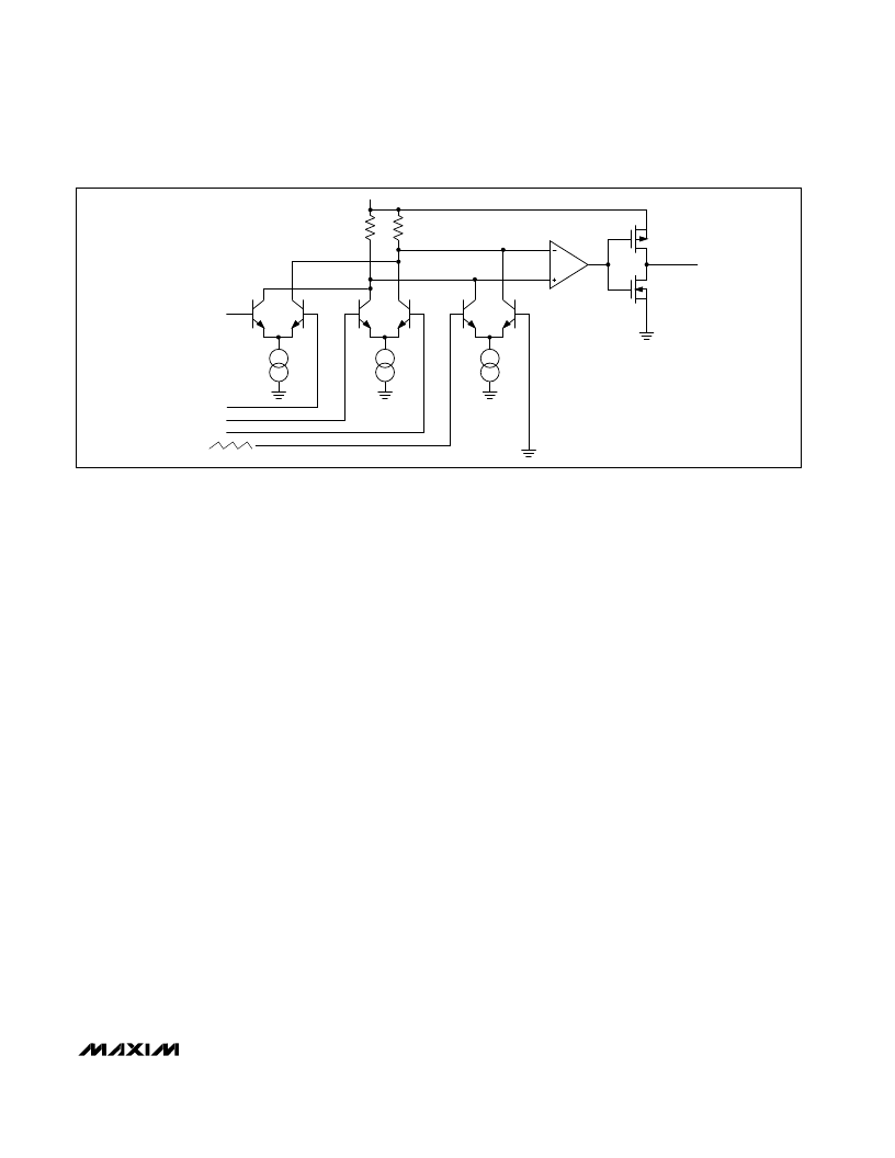
FB
REF
CSH
CSL
SLOPE COMPENSATION
VL
I1
R1
R2
TO PWM
LOGIC
OUTPUT DRIVER
UNCOMPENSATED
HIGH-SPEED
LEVEL TRANSLATOR
AND BUFFER
I2
I3
Figure 4. Main PWM Comparator Block Diagram
相关PDF资料 |
PDF描述 |
|---|---|
| MAX1653 | High-Efficiency, PWM, Step-Down DC-DC Controllers in 16-Pin QSOP |
| MAX1654 | High-Efficiency, PWM, Step-Down DC-DC Controllers in 16-Pin QSOP |
| MAX1655 | High-Efficiency, PWM, Step-Down DC-DC Controllers in 16-Pin QSOP |
| MAX1655EEE | High-Efficiency, PWM, Step-Down DC-DC Controllers in 16-Pin QSOP |
| MAX1653EEE | High-Efficiency, PWM, Step-Down DC-DC Controllers in 16-Pin QSOP |
相关代理商/技术参数 |
参数描述 |
|---|---|
| MAX1652EEE+ | 功能描述:DC/DC 开关控制器 PWM Step-Down RoHS:否 制造商:Texas Instruments 输入电压:6 V to 100 V 开关频率: 输出电压:1.215 V to 80 V 输出电流:3.5 A 输出端数量:1 最大工作温度:+ 125 C 安装风格: 封装 / 箱体:CPAK |
| MAX1652EEE+T | 功能描述:DC/DC 开关控制器 PWM Step-Down RoHS:否 制造商:Texas Instruments 输入电压:6 V to 100 V 开关频率: 输出电压:1.215 V to 80 V 输出电流:3.5 A 输出端数量:1 最大工作温度:+ 125 C 安装风格: 封装 / 箱体:CPAK |
| MAX1652EEE-T | 功能描述:DC/DC 开关控制器 RoHS:否 制造商:Texas Instruments 输入电压:6 V to 100 V 开关频率: 输出电压:1.215 V to 80 V 输出电流:3.5 A 输出端数量:1 最大工作温度:+ 125 C 安装风格: 封装 / 箱体:CPAK |
| MAX1653EEE | 功能描述:DC/DC 开关控制器 PWM Step-Down RoHS:否 制造商:Texas Instruments 输入电压:6 V to 100 V 开关频率: 输出电压:1.215 V to 80 V 输出电流:3.5 A 输出端数量:1 最大工作温度:+ 125 C 安装风格: 封装 / 箱体:CPAK |
| MAX1653EEE+ | 功能描述:DC/DC 开关控制器 PWM Step-Down RoHS:否 制造商:Texas Instruments 输入电压:6 V to 100 V 开关频率: 输出电压:1.215 V to 80 V 输出电流:3.5 A 输出端数量:1 最大工作温度:+ 125 C 安装风格: 封装 / 箱体:CPAK |
发布紧急采购,3分钟左右您将得到回复。