- 您现在的位置:买卖IC网 > PDF目录383330 > MAX1654EEE (MAXIM INTEGRATED PRODUCTS INC) High-Efficiency, PWM, Step-Down DC-DC Controllers in 16-Pin QSOP PDF资料下载
参数资料
| 型号: | MAX1654EEE |
| 厂商: | MAXIM INTEGRATED PRODUCTS INC |
| 元件分类: | 稳压器 |
| 英文描述: | High-Efficiency, PWM, Step-Down DC-DC Controllers in 16-Pin QSOP |
| 中文描述: | SWITCHING CONTROLLER, 350 kHz SWITCHING FREQ-MAX, PDSO16 |
| 封装: | 0.150 INCH, 0.025 INCH PITCH, QSOP-16 |
| 文件页数: | 16/28页 |
| 文件大小: | 265K |
| 代理商: | MAX1654EEE |
第1页第2页第3页第4页第5页第6页第7页第8页第9页第10页第11页第12页第13页第14页第15页当前第16页第17页第18页第19页第20页第21页第22页第23页第24页第25页第26页第27页第28页
M
High-Effic ienc y, PWM, S tep-Down
DC-DC Controllers in 16-Pin QS OP
16
______________________________________________________________________________________
an action that “boosts” the 5V gate-drive signal above
the battery voltage.
Ringing seen at the high-side MOSFET gate (DH) in
discontinuous-conduction mode (light loads) is a natur-
al operating condition caused by the residual energy in
the tank circuit formed by the inductor and stray capac-
itance at the switching node LX. The gate-driver nega-
tive rail is referred to LX, so any ringing there is directly
coupled to the gate-drive output.
Current-Limiting and
Current-S ense Inputs (CS H and CS L)
The current-limit circuit resets the main PWM latch and
turns off the high-side MOSFET switch whenever the
voltage difference between CSH and CSL exceeds
100mV. This limiting is effective for both current flow
directions, putting the threshold limit at ±100mV. The
tolerance on the positive current limit is ±20%, so the
external low-value sense resistor must be sized for
80mV/R1 to guarantee enough load capability, while
components must be designed to withstand continuous
current stresses of 120mV/R1.
For breadboarding purposes or very-high-current appli-
cations, it may be useful to wire the current-sense inputs
with a twisted pair rather than PC traces.
Osc illator Frequenc y and
S ync hronization (S Y NC Pin)
The SYNC input controls the oscillator frequency.
Connecting SYNC to GND or to VL selects 150kHz
operation; connecting SYNC to REF selects 300kHz.
SYNC can also be used to synchronize with an external
5V CMOS clock generator. SYNC has a guaranteed
190kHz to 340kHz capture range.
300kHz operation optimizes the application circuit for
component size and cost. 150kHz operation provides
increased efficiency and improved low-duty factor
operation (see Dropout Operationsection).
Dropout Operation
Dropout (low input-output differential operation) is en-
hanced by stretching the clock pulse width to increase
the maximum duty factor. The algorithm follows: if the out-
put voltage (V
OUT
) drops out of regulation without the
current limit having been reached, the controller skips an
off-time period (extending the on-time). At the end of the
cycle, if the output is still out of regulation, another off-time
period is skipped. This action can continue until three off-
time periods are skipped, effectively dividing the clock
frequency by as much as four.
The typical PWM minimum off-time is 300ns, regardless
of the operating frequency. Lowering the operating fre-
quency raises the maximum duty factor above 98%.
Low-Noise Mode (S K IP Pin)
The low-noise mode (SKIP = high) is useful for minimiz-
ing RF and audio interference in noise-sensitive appli-
cations such as audio-equipped systems, cellular
phones, RF communicating computers, and electro-
magnetic pen-entry systems. See the summary of oper-
ating modes in Table 3. SKIP can be driven from an
external logic signal.
The MAX1653 and MAX1655 can reduce interference
due to switching noise by ensuring a constant switch-
ing frequency regardless of load and line conditions,
thus concentrating the emissions at a known frequency
outside the system audio or IF bands. Choose an oscil-
lator frequency where harmonics of the switching fre-
quency don’t overlap a sensitive frequency band. If
necessary, synchronize the oscillator to a tight-toler-
ance external clock generator.
The low-noise mode (SKIP = high) forces two changes
upon the PWM controller. First, it ensures fixed-frequen-
cy operation by disabling the minimum-current com-
parator and ensuring that the PWM latch is set at the
beginning of each cycle, even if the output is in regula-
tion. Second, it ensures continuous inductor current
MAX1652
MAX1653
MAX1654
MAX1655
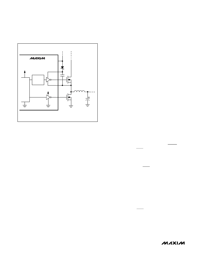
BST
VL
+5V
VL SUPPLY
BATTERY
INPUT
VL
VL
DH
LX
DL
PWM
LEVEL
TRANSLATOR
Figure 5. Boost Supply for Gate Drivers
相关PDF资料 |
PDF描述 |
|---|---|
| MAX1658 | 350mA, 16.5V Input, Low-Dropout Linear Regulators |
| MAX1658ESA | 350mA, 16.5V Input, Low-Dropout Linear Regulators |
| MAX1659ESA | 350mA, 16.5V Input, Low-Dropout Linear Regulators |
| MAX165ACPN | CMOS レP-Compatible, 5レs, 8-Bit ADCs |
| MAX166DCPP | CMOS レP-Compatible, 5レs, 8-Bit ADCs |
相关代理商/技术参数 |
参数描述 |
|---|---|
| MAX1654EEE+ | 功能描述:DC/DC 开关控制器 PWM Step-Down RoHS:否 制造商:Texas Instruments 输入电压:6 V to 100 V 开关频率: 输出电压:1.215 V to 80 V 输出电流:3.5 A 输出端数量:1 最大工作温度:+ 125 C 安装风格: 封装 / 箱体:CPAK |
| MAX1654EEE+T | 功能描述:DC/DC 开关控制器 PWM Step-Down RoHS:否 制造商:Texas Instruments 输入电压:6 V to 100 V 开关频率: 输出电压:1.215 V to 80 V 输出电流:3.5 A 输出端数量:1 最大工作温度:+ 125 C 安装风格: 封装 / 箱体:CPAK |
| MAX1654EEE-T | 功能描述:DC/DC 开关控制器 PWM Step-Down RoHS:否 制造商:Texas Instruments 输入电压:6 V to 100 V 开关频率: 输出电压:1.215 V to 80 V 输出电流:3.5 A 输出端数量:1 最大工作温度:+ 125 C 安装风格: 封装 / 箱体:CPAK |
| MAX1655EEE | 功能描述:DC/DC 开关控制器 PWM Step-Down RoHS:否 制造商:Texas Instruments 输入电压:6 V to 100 V 开关频率: 输出电压:1.215 V to 80 V 输出电流:3.5 A 输出端数量:1 最大工作温度:+ 125 C 安装风格: 封装 / 箱体:CPAK |
| MAX1655EEE+ | 功能描述:DC/DC 开关控制器 PWM Step-Down RoHS:否 制造商:Texas Instruments 输入电压:6 V to 100 V 开关频率: 输出电压:1.215 V to 80 V 输出电流:3.5 A 输出端数量:1 最大工作温度:+ 125 C 安装风格: 封装 / 箱体:CPAK |
发布紧急采购,3分钟左右您将得到回复。