- 您现在的位置:买卖IC网 > PDF目录383330 > MAX1655 (Maxim Integrated Products, Inc.) High-Efficiency, PWM, Step-Down DC-DC Controllers in 16-Pin QSOP PDF资料下载
参数资料
| 型号: | MAX1655 |
| 厂商: | Maxim Integrated Products, Inc. |
| 英文描述: | High-Efficiency, PWM, Step-Down DC-DC Controllers in 16-Pin QSOP |
| 中文描述: | 高效率、PWM、降压型DC-DC控制器,16引脚QSOP封装 |
| 文件页数: | 10/28页 |
| 文件大小: | 265K |
| 代理商: | MAX1655 |
第1页第2页第3页第4页第5页第6页第7页第8页第9页当前第10页第11页第12页第13页第14页第15页第16页第17页第18页第19页第20页第21页第22页第23页第24页第25页第26页第27页第28页
M
High-Effic ienc y, PWM, S tep-Down
DC-DC Controllers in 16-Pin QS OP
10
______________________________________________________________________________________
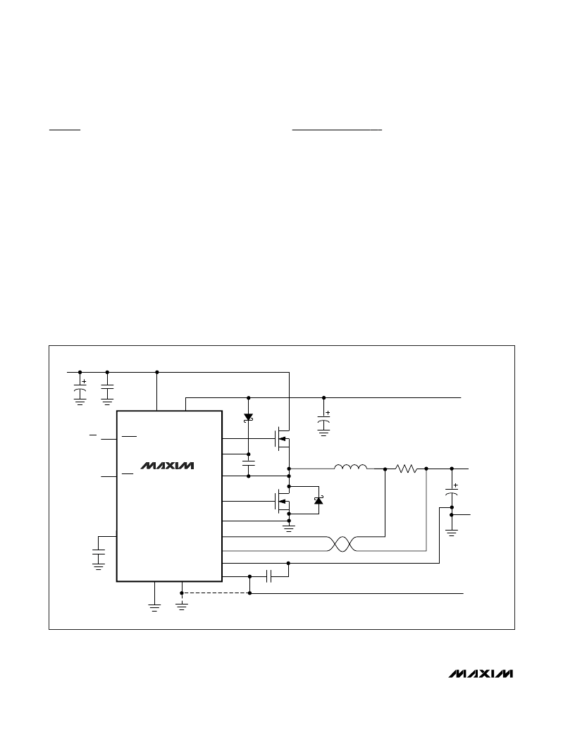
S tandard Applic ation Circ uits
It’s easy to adapt the basic MAX1653 single-output 3.3V
buck converter (Figure 1) to meet a wide range of appli-
cations with inputs up to 30V (limited by choice of exter-
nal MOSFET). Simply substitute the appropriate
components from Table 1 (candidate suppliers are pro-
vided in Table 2). These circuits represent a good set of
trade-offs among cost, size, and efficiency while staying
within the worst-case specification limits for stress-relat-
ed parameters such as capacitor ripple current.
Don’t change the frequency of these circuits without
first recalculating component values (particularly induc-
tance value at maximum battery voltage).
For a discussion of dual-output circuits using the
MAX1652 and MAX1654, see Figure 9 and the
Secondary Feedback-Regulation Loop section.
Detailed Desc ription
The MAX1652 family are BiCMOS, switch-mode power-
supply controllers designed primarily for buck-topology
regulators in battery-powered applications where high
efficiency and low quiescent supply current are critical.
The parts also work well in other topologies such as
boost, inverting, and Cuk due to the flexibility of their
floating high-speed gate driver. Light-load efficiency is
enhanced by automatic idle-mode operation—a vari-
able-frequency pulse-skipping mode that reduces
losses due to MOSFET gate charge. The step-down
power-switching circuit consists of two N-channel
MOSFETs, a rectifier, and an LC output filter. The out-
put voltage is the average of the AC voltage at the
switching node, which is adjusted and regulated by
changing the duty cycle of the MOSFET switches. The
gate-drive signal to the N-channel high-side MOSFET
must exceed the battery voltage and is provided by a
flying capacitor boost circuit that uses a 100nF capaci-
tor connected to BST.
MAX1653
CSL
CSH
VL
SYNC
5
FB
7
V+
10
11
14
Q1
Q2
16
15
13
D2
CMPSH-3
J1
150kHz/300kHz
JUMPER
NOTE:
KEEP CURRENT-SENSE
LINES SHORT AND CLOSE
TOGETHER. SEE FIGURE 8.
D1
12
8
9
REF
3
GND
4
+5V AT
5mA
+3.3V
OUTPUT
GND
OUT
BST
DH
LX
DL
2
1
LOW-NOISE
CONTROL
PGND
SKIP
SS
6
ON/OFF
CONTROL
SHDN
INPUT
REF OUTPUT
+2.5V AT 100
μ
A
C5
0.33
μ
F
C4
4.7
μ
F
C7
0.1
μ
F
C6
0.01
μ
F
(OPTIONAL)
C1
C2
C3
0.1
μ
F
R1
L1
Figure 1. Standard 3.3V Application Circuit (see Table 1 for Component Values)
相关PDF资料 |
PDF描述 |
|---|---|
| MAX1655EEE | High-Efficiency, PWM, Step-Down DC-DC Controllers in 16-Pin QSOP |
| MAX1653EEE | High-Efficiency, PWM, Step-Down DC-DC Controllers in 16-Pin QSOP |
| MAX1654EEE | High-Efficiency, PWM, Step-Down DC-DC Controllers in 16-Pin QSOP |
| MAX1658 | 350mA, 16.5V Input, Low-Dropout Linear Regulators |
| MAX1658ESA | 350mA, 16.5V Input, Low-Dropout Linear Regulators |
相关代理商/技术参数 |
参数描述 |
|---|---|
| MAX1655EEE | 功能描述:DC/DC 开关控制器 PWM Step-Down RoHS:否 制造商:Texas Instruments 输入电压:6 V to 100 V 开关频率: 输出电压:1.215 V to 80 V 输出电流:3.5 A 输出端数量:1 最大工作温度:+ 125 C 安装风格: 封装 / 箱体:CPAK |
| MAX1655EEE+ | 功能描述:DC/DC 开关控制器 PWM Step-Down RoHS:否 制造商:Texas Instruments 输入电压:6 V to 100 V 开关频率: 输出电压:1.215 V to 80 V 输出电流:3.5 A 输出端数量:1 最大工作温度:+ 125 C 安装风格: 封装 / 箱体:CPAK |
| MAX1655EEE+T | 功能描述:DC/DC 开关控制器 PWM Step-Down RoHS:否 制造商:Texas Instruments 输入电压:6 V to 100 V 开关频率: 输出电压:1.215 V to 80 V 输出电流:3.5 A 输出端数量:1 最大工作温度:+ 125 C 安装风格: 封装 / 箱体:CPAK |
| MAX1655EEE-T | 功能描述:DC/DC 开关控制器 PWM Step-Down RoHS:否 制造商:Texas Instruments 输入电压:6 V to 100 V 开关频率: 输出电压:1.215 V to 80 V 输出电流:3.5 A 输出端数量:1 最大工作温度:+ 125 C 安装风格: 封装 / 箱体:CPAK |
| MAX1655ESE | 功能描述:DC/DC 开关控制器 PWM Step-Down RoHS:否 制造商:Texas Instruments 输入电压:6 V to 100 V 开关频率: 输出电压:1.215 V to 80 V 输出电流:3.5 A 输出端数量:1 最大工作温度:+ 125 C 安装风格: 封装 / 箱体:CPAK |
发布紧急采购,3分钟左右您将得到回复。