- 您现在的位置:买卖IC网 > PDF目录20745 > MAX1659ESA (Maxim Integrated)IC REG LDO 5V/ADJ .35A 8-SOIC PDF资料下载
参数资料
| 型号: | MAX1659ESA |
| 厂商: | Maxim Integrated |
| 文件页数: | 8/12页 |
| 文件大小: | 0K |
| 描述: | IC REG LDO 5V/ADJ .35A 8-SOIC |
| 产品培训模块: | Lead (SnPb) Finish for COTS Obsolescence Mitigation Program |
| 标准包装: | 100 |
| 稳压器拓扑结构: | 正,固定式或可调式 |
| 输出电压: | 5V,1.25 V ~ 16 V |
| 输入电压: | 2.7 V ~ 16.5 V |
| 电压 - 压降(标准): | 0.49V @ 350mA |
| 稳压器数量: | 1 |
| 电流 - 输出: | 350mA(最小) |
| 工作温度: | -40°C ~ 85°C |
| 安装类型: | 表面贴装 |
| 封装/外壳: | 8-SOIC(0.154",3.90mm 宽) |
| 供应商设备封装: | 8-SOIC |
| 包装: | 管件 |
�� �
�
�350mA,� 16.5V� Input,�
�Low-Dropout� Linear� Regulators�
�Thermal-Overload� Protection�
�Thermal-overload� protection� limits� total� power� dissipa-�
�tion� in� the� MAX1658/MAX1659.� When� the� junction� tem-�
�1600�
�perature� exceeds� T� J� =� +165°C,� the� pass� transistor�
�deactivates,� allowing� the� IC� to� cool.� Once� it� has� cooled�
�by� 10°C,� the� control� logic� will� enable� operation.� Under�
�thermal� overload,� the� output� of� the� device� will� pulse� as�
�the� die� heats� up� and� then� cools� to� operational� levels.�
�Prolonged� operation� under� these� conditions� is� not� rec-�
�ommended.�
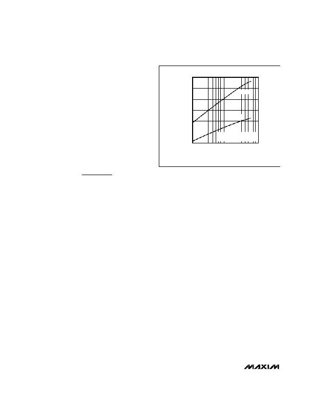
�Operating� Region� and� Power� Dissipation�
�Maximum� power� dissipation� of� the� MAX1658/MAX1659�
�depends� on� the� thermal� resistance� of� the� package� and�
�circuit� board,� the� temperature� difference� between� the�
�1400�
�1200�
�1000�
�800�
�600�
�400�
�T� j� = +125°C�
�T� j� =� +85°C�
�SINGLE-SIDED� 1oz.� COPPER�
�T� A� =� +25°C,� STILL� AIR�
�die� and� ambient� air,� and� the� rate� of� air� flow.� The� power�
�dissipation� by� the� device� is� P� =� I� OUT� (V� IN� -� V� OUT� ).� The�
�maximum� power� dissipation� is:�
�0.1�
�0.65�
�1�
�6.5�
�COPPER� GROUND� PAD� AREA�
�10� (in� 2� )�
�65� (cm� 2� )�
�(�
�(�
�?� θ�
�??�
�?�
�P� MAX� =� ?�
�?�
�T� J� ?� T� A� )�
�JB� +� θ� BA�
�)�
�?�
�?�
�Figure� 4.� Typical� Maximum� Power� Dissipation� vs.� Ground� Pad�
�Area�
�P� MAX� x� (� 125� °� C� ?� T� A� )�
�(�
�)�
�I� OUT� (� MAX� )� =�
�where� (T� J� -� T� A� )� is� the� temperature� difference� between�
�MAX1658/MAX1659� die� junction� and� the� surrounding�
�air,� θ� JB� is� the� thermal� resistance� of� the� package,� and�
�θ� BA� is� the� thermal� resistance� through� the� printed� circuit�
�board,� copper� traces,� and� other� materials� to� the�
�surrounding� air.� The� 8-pin� SO� package� for� the�
�MAX1658/MAX1659� features� a� special� lead� frame� with�
�a� lower� thermal� resistance� and� higher� allowable� power�
�dissipation� than� a� standard� SO-8.� The� thermal� resis-�
�tance� of� this� package� is� θ� JB� =� 69°C/W,� compared� with�
�θ� JB� =� 170°C/W� for� an� SO-8.�
�The� IN� pins� of� the� MAX1658/MAX1659� package� per-�
�form� the� dual� function� of� providing� an� electrical� con-�
�nection� to� IN� and� channeling� heat� away.� Connect� all� IN�
�pins� to� the� input� voltage� using� a� large� pad� or� power�
�plane� on� the� surface.� Where� this� is� impossible,� connect�
�to� a� copper� plane� on� an� adjacent� layer.� The� pad� should�
�meet� the� dimensions� specified� in� Figure� 4.�
�Figure� 4� assumes� the� IC� is� soldered� directly� to� the� pad,�
�has� a� +125°C� maximum� junction� temperature� and� a�
�+25°C� ambient� air� temperature,� and� has� no� other� heat�
�sources.� Use� larger� pad� sizes� for� lower� junction� tem-�
�peratures,� higher� ambient� temperatures,� or� conditions�
�where� the� IC� is� not� soldered� directly� to� a� heat-sinking�
�IN� pad.�
�The� MAX1658/MAX1659� can� regulate� currents� up� to�
�350mA� and� operate� with� input� voltages� up� to� 16.5V,� but�
�not� simultaneously.� High� output� currents� can� only� be�
�sustained� when� input-output� differential� voltage� is� low,�
�as� shown� in� the� following� equation.� Maximum� power�
�dissipation� depends� on� packaging,� board� layout,� tem-�
�perature,� and� air� flow.� The� maximum� output� current� is:�
�V� IN� ?� V� OUT� x� 100� °� C�
�where� P� MAX� is� derived� from� the� T� J� =� 125°C� curve� of�
�Figure� 4.�
�Reverse� Battery� Protection�
�The� MAX1658/MAX1659� feature� reverse� battery� protec-�
�tion.� Under� normal� operation,� a� P-channel� MOSFET�
�connects� the� substrate� of� the� device� to� IN.� When� the�
�input� voltage� falls� below� ground� (implying� reverse� bat-�
�tery� conditions),� the� P-channel� switch� turns� off� and� dis-�
�connects� the� substrate� from� IN,� disabling� the� device.�
�The� maximum� reverse� battery� voltage� allowed� is� -17V.�
�SHDN� also� withstands� reverse� battery� conditions� and�
�can� be� connected� directly� to� IN� with� no� loss� of� protec-�
�tion.�
�Polarized� input� bypass� capacitors� will� be� damaged�
�under� reverse� battery� conditions.� To� ensure� circuit� reli-�
�ability,� use� a� non-polarized� capacitor� at� the� input.�
�The� MAX1658/MAX1659� do� not� provide� reverse� current�
�protection.� If� V� OUT� is� greater� than� V� IN� by� more� than�
�300mV,� reverse� current� will� flow.� Reverse� current� pro-�
�tection� can� be� added� by� connecting� a� Schottky� diode�
�in� series� with� IN.�
�8�
�_______________________________________________________________________________________�
�相关PDF资料 |
PDF描述 |
|---|---|
| ABM40DTKI | CONN EDGECARD 80POS DIP .156 SLD |
| EB43-S4R4060W | CONN EDGEBOARD DUAL 80POS 3A |
| GBC30DCSH | CONN EDGECARD 60POS DIP .100 SLD |
| EBM08DRSN-S288 | CONN EDGECARD 16POS .156 EXTEND |
| VI-J2N-CX-F3 | CONVERTER MOD DC/DC 18.5V 75W |
相关代理商/技术参数 |
参数描述 |
|---|---|
| MAX1659ESA+ | 功能描述:低压差稳压器 - LDO 350mA 16.5V RoHS:否 制造商:Texas Instruments 最大输入电压:36 V 输出电压:1.4 V to 20.5 V 回动电压(最大值):307 mV 输出电流:1 A 负载调节:0.3 % 输出端数量: 输出类型:Fixed 最大工作温度:+ 125 C 安装风格:SMD/SMT 封装 / 箱体:VQFN-20 |
| MAX1659ESA+T | 功能描述:低压差稳压器 - LDO 350mA 16.5V RoHS:否 制造商:Texas Instruments 最大输入电压:36 V 输出电压:1.4 V to 20.5 V 回动电压(最大值):307 mV 输出电流:1 A 负载调节:0.3 % 输出端数量: 输出类型:Fixed 最大工作温度:+ 125 C 安装风格:SMD/SMT 封装 / 箱体:VQFN-20 |
| MAX1659ESA-T | 功能描述:低压差稳压器 - LDO 350mA 16.5V RoHS:否 制造商:Texas Instruments 最大输入电压:36 V 输出电压:1.4 V to 20.5 V 回动电压(最大值):307 mV 输出电流:1 A 负载调节:0.3 % 输出端数量: 输出类型:Fixed 最大工作温度:+ 125 C 安装风格:SMD/SMT 封装 / 箱体:VQFN-20 |
| MAX165ACPN | 功能描述:模数转换器 - ADC Integrated Circuits (ICs) RoHS:否 制造商:Texas Instruments 通道数量:2 结构:Sigma-Delta 转换速率:125 SPs to 8 KSPs 分辨率:24 bit 输入类型:Differential 信噪比:107 dB 接口类型:SPI 工作电源电压:1.7 V to 3.6 V, 2.7 V to 5.25 V 最大工作温度:+ 85 C 安装风格:SMD/SMT 封装 / 箱体:VQFN-32 |
| MAX165ACPN+ | 功能描述:模数转换器 - ADC 8-Bit 200ksps 2.46V Precision ADC RoHS:否 制造商:Texas Instruments 通道数量:2 结构:Sigma-Delta 转换速率:125 SPs to 8 KSPs 分辨率:24 bit 输入类型:Differential 信噪比:107 dB 接口类型:SPI 工作电源电压:1.7 V to 3.6 V, 2.7 V to 5.25 V 最大工作温度:+ 85 C 安装风格:SMD/SMT 封装 / 箱体:VQFN-32 |
发布紧急采购,3分钟左右您将得到回复。