- 您现在的位置:买卖IC网 > Datasheet目录989 > MAX16809EVKIT+ (Maxim Integrated Products)EVAL KIT FOR MAX16809 Datasheet资料下载
参数资料
| 型号: | MAX16809EVKIT+ |
| 厂商: | Maxim Integrated Products |
| 文件页数: | 13/20页 |
| 文件大小: | 0K |
| 描述: | EVAL KIT FOR MAX16809 |
| 标准包装: | 1 |
| 电流 - 输出 / 通道: | 40mA |
| 输出及类型: | 16,非隔离 |
| 输出电压: | 32V |
| 特点: | 可调光 |
| 输入电压: | 9 ~ 16 V |
| 已供物品: | 板 |
| 已用 IC / 零件: | MAX16809 |
�� �
�
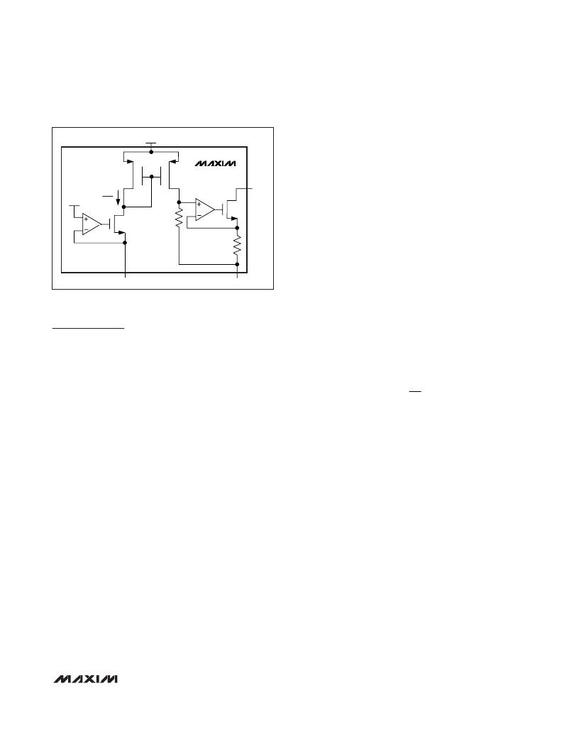
�Integrated� 16-Channel� LED� Driver� with�
�Switch-Mode� Boost� and� SEPIC� Controller�
�V+�
�MAX16809�
�pMOS� typically� 3.5� Ω� and� the� on-resistance� of� the� nMOS�
�typically� 4.5� Ω� .� The� driver� can� source� 2A� and� sink� 1A� typi-�
�cally.� This� allows� for� the� MAX16809� to� quickly� turn� on� and�
�off� high� gate-charge� MOSFETs.� Bypass� V� CC� with� one� or�
�more� 0.1μF� ceramic� capacitors� to� AGND,� placed� close� to�
�1.23V�
�1.23�
�R� EST�
�68W/L�
�W/L�
�945R�
�OUT_� _�
�V� CC� .� The� average� current� sourced� to� drive� the� external�
�MOSFET� depends� on� the� total� gate� charge� (Q� G� )� and�
�operating� frequency� of� the� converter.� The� power� dissipa-�
�tion� in� the� MAX16809� is� a� function� of� the� average� output�
�drive� current� (I� DRIVE� ).� Use� the� following� equation� to� cal-�
�culate� the� power� dissipation� in� the� device� due� to� I� DRIVE� :�
�R�
�I� DRIVE� =� (Q� G� x� f� SW� )�
�PD� =� (I� DRIVE� +� I� CC� )� x� V� CC�
�where� I� CC� is� the� operating� supply� current.� See� the�
�SET�
�PGND�
�Typical� Operating� Characteristics� for� the� operating�
�supply� current� at� a� given� frequency.�
�Figure� 1b.� OUT_� _� Driver� Internal� Diagram�
�Error� Amplifier�
�Switch-Mode� Controller�
�Current-Mode� Control� Loop�
�The� advantages� of� current-mode� control� over� voltage-�
�mode� control� are� twofold.� First,� there� is� the� feed-for-�
�ward� characteristic� brought� on� by� the� controller’s� ability�
�The� MAX16809� includes� an� internal� error� amplifier.� The�
�inverting� input� is� at� FB� and� the� noninverting� input� is�
�internally� connected� to� a� 2.5V� reference.� Set� the� output�
�voltage� using� a� resistive� divider� between� output� of� the�
�converter� V� OUT� ,� FB,� and� AGND.� Use� the� following� for-�
�mula� to� set� the� output� voltage:�
�V� OUT� =� ?� 1� +�
�to adjust for variations in the input voltage on a cycle-�
�by-cycle� basis.� Second,� the� stability� requirements� of�
�the� current-mode� controller� are� reduced� to� that� of� a� sin-�
�?�
�?�
�R1� ?�
�R� 2� ?� ?�
�x� V� FB�
�gle-pole� system� unlike� the� double� pole� in� the� voltage-�
�mode� control� scheme.� The� MAX16809� uses� a�
�current-mode� control� loop� where� the� output� of� the� error�
�amplifier� is� compared� to� the� current-sense� voltage�
�(V� CS� ).� When� the� current-sense� signal� is� lower� than� the�
�inverting� input� of� the� CPWM� comparator,� the� output� of�
�the� comparator� is� low� and� the� switch� is� turned� on� at�
�each� clock� pulse.� When� the� current-sense� signal� is�
�higher� than� the� inverting� input� of� the� CPWM� compara-�
�tor,� the� output� is� high� and� the� switch� is� turned� off.�
�Undervoltage� Lockout� (UVLO)�
�The� turn-on� supply� voltage� for� the� MAX16809� is� 8.4V�
�(typ).� Once� V� CC� reaches� 8.4V,� the� reference� powers� up.�
�There� is� a� 0.8V� of� hysteresis� from� the� turn-on� voltage� to�
�the� UVLO� threshold.� Once� V� CC� reaches� 8.4V,� the�
�MAX16809� operates� with� V� CC� down� to� 7.6V.� Once� V� CC�
�goes� below� 7.6V� (typ),� the� device� is� in� UVLO.� When� in�
�UVLO,� the� quiescent� supply� current� into� V� CC� falls� back�
�to� 32μA� (typ),� and� OUT� and� REF� are� pulled� low.�
�MOSFET� Driver�
�OUT� drives� an� external� n-channel� MOSFET� and� swings�
�from� AGND� to� V� CC� .� Ensure� that� V� CC� remains� below� the�
�absolute� maximum� V� GS� rating� of� the� external� MOSFET.�
�OUT� is� a� push-pull� output� with� the� on-resistance� of� the�
�where� V� FB� =� 2.5V.�
�Oscillator�
�The� oscillator� frequency� is� programmable� using� an�
�external� capacitor� and� a� resistor� at� RTCT� (see� R� T� and�
�C� T� in� the� Typical� Operating� Circuits).� R� T� is� connected�
�from� RTCT� to� the� 5V� reference� (REF),� and� C� T� is� con-�
�nected� from� RTCT� to� AGND.� REF� charges� C� T� through�
�R� T� until� its� voltage� reaches� 2.8V.� C� T� then� discharges�
�through� an� 8.3mA� internal� current� sink� until� C� T� ’s� voltage�
�reaches� 1.1V,� at� which� time� C� T� is� allowed� to� charge�
�through� R� T� again.� The� oscillator’s� period� is� the� sum� of�
�the� charge� and� discharge� times� of� C� T� .� Calculate� the�
�charge� time� as� follows:�
�t� C� =� 0.57� x� R� T� x� C� T�
�where� t� C� is� in� seconds,� R� T� in� ohms� (� Ω� ),� and� C� T� in�
�Farads� (F).�
�The� discharge� time� is� then:�
�t� D� =� (R� T� x� C� T� x� 1000)� /� [(4.88� x� R� T� )� -� (1.8� x� 1000)]�
�where� t� D� is� in� seconds,� R� T� in� ohms� (� Ω� ),� and� C� T� in�
�Farads� (F).�
�______________________________________________________________________________________�
�13�
�相关PDF资料 |
PDF描述 |
|---|---|
| MAX16814EVKIT+ | KIT EAL FOR MAX16814 |
| MAX16816EVKIT+ | KIT EVAL FOR MAX16816 LED DRIVER |
| MAX16818EVKIT+ | KIT EVALUATION FOR MAX16818 |
| MAX16820EVKIT+ | EVAL KIT FOR MAX16820 |
| MAX16821BEVKIT+ | KIT EVAL FOR MAX16821B |
相关代理商/技术参数 |
参数描述 |
|---|---|
| MAX16809EVKIT+ | 功能描述:LED 照明开发工具 MAX16809 Eval Kit RoHS:否 制造商:Fairchild Semiconductor 产品:Evaluation Kits 用于:FL7732 核心: 电源电压:120V 系列: 封装: |
| MAX1680C/D | 功能描述:直流/直流开关转换器 DICE SALES DICE RoHS:否 制造商:STMicroelectronics 最大输入电压:4.5 V 开关频率:1.5 MHz 输出电压:4.6 V 输出电流:250 mA 输出端数量:2 最大工作温度:+ 85 C 安装风格:SMD/SMT |
| MAX1680ESA | 功能描述:直流/直流开关转换器 125mA f-Selct Swtchd Cap Volt Converter RoHS:否 制造商:STMicroelectronics 最大输入电压:4.5 V 开关频率:1.5 MHz 输出电压:4.6 V 输出电流:250 mA 输出端数量:2 最大工作温度:+ 85 C 安装风格:SMD/SMT |
| MAX1680ESA+ | 功能描述:直流/直流开关转换器 125mA f-Selct Swtchd Cap Volt Converter RoHS:否 制造商:STMicroelectronics 最大输入电压:4.5 V 开关频率:1.5 MHz 输出电压:4.6 V 输出电流:250 mA 输出端数量:2 最大工作温度:+ 85 C 安装风格:SMD/SMT |
| MAX1680ESA+T | 功能描述:直流/直流开关转换器 125mA f-Selct Swtchd Cap Volt Converter RoHS:否 制造商:STMicroelectronics 最大输入电压:4.5 V 开关频率:1.5 MHz 输出电压:4.6 V 输出电流:250 mA 输出端数量:2 最大工作温度:+ 85 C 安装风格:SMD/SMT |
发布紧急采购,3分钟左右您将得到回复。