- 您现在的位置:买卖IC网 > Datasheet目录989 > MAX16818EVKIT+ (Maxim Integrated Products)KIT EVALUATION FOR MAX16818 Datasheet资料下载
参数资料
| 型号: | MAX16818EVKIT+ |
| 厂商: | Maxim Integrated Products |
| 文件页数: | 24/25页 |
| 文件大小: | 0K |
| 描述: | KIT EVALUATION FOR MAX16818 |
| 产品培训模块: | Lead (SnPb) Finish for COTS Obsolescence Mitigation Program |
| 标准包装: | 1 |
| 电流 - 输出 / 通道: | 1A |
| 输出及类型: | 1,非隔离 |
| 输出电压: | 18V |
| 特点: | 可调光 |
| 输入电压: | 6 ~ 28 V |
| 已供物品: | 板 |
| 已用 IC / 零件: | MAX16818 |
�� �
�
�1.5MHz,� 30A� High-Efficiency,� LED� Driver�
�with� Rapid� LED� Current� Pulsing�
�PCB� Layout� Guidelines�
�Use� the� following� guidelines� to� layout� the� switching� volt-�
�age� regulator:�
�1)� Place� the� IN,� V� CC� ,� and� V� DD� bypass� capacitors�
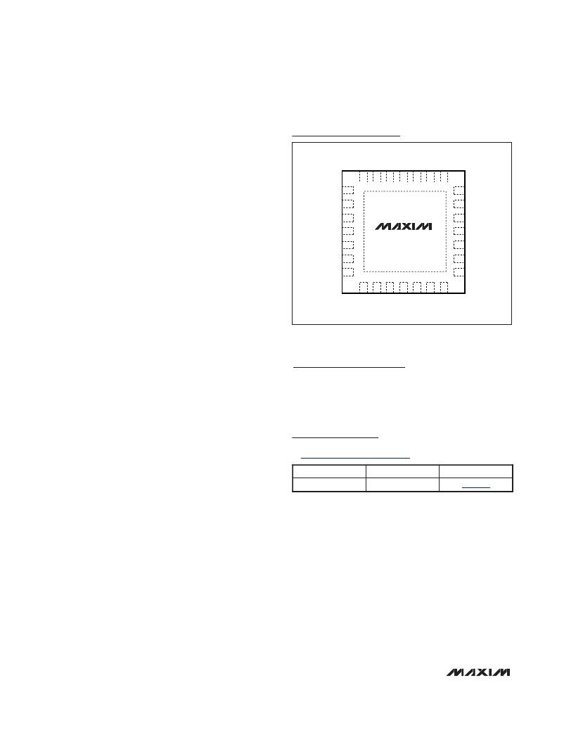
�TOP� VIEW�
�Pin� Configuration�
�close� to� the� MAX16818.�
�21�
�20�
�19�
�18�
�17�
�16�
�15�
�2)� Minimize� the� area� and� length� of� the� high� current�
�loops� from� the� input� capacitor,� upper� switching�
�MOSFET,� inductor,� and� output� capacitor� back� to�
�the� input� capacitor� negative� terminal.�
�SGND�
�SENSE-�
�SENSE+�
�22�
�23�
�24�
�14�
�13�
�12�
�LIM�
�V_IOUT�
�RT/SYNC�
�3)� Keep� short� the� current� loop� formed� by� the� lower�
�switching� MOSFET,� inductor,� and� output� capacitor.�
�SGND�
�IN�
�25�
�26�
�MAX16818�
�11�
�10�
�EN�
�PGOOD�
�4)� Place� the� Schottky� diodes� close� to� the� lower�
�MOSFETs� and� on� the� same� side� of� the� PCB.�
�5)� Keep� the� SGND� and� PGND� isolated� and� connect�
�them� at� one� single� point.�
�V� CC�
�V� DD�
�27�
�28�
�+�
�1�
�*� EXPOSED� PAD�
�2� 3�
�4�
�5�
�6�
�7�
�9�
�8�
�CLKOUT�
�SGND�
�6)� Run� the� current-sense� lines� CSP� and� CSN� very�
�close� to� each� other� to� minimize� the� loop� area.�
�Similarly,� run� the� remote� voltage-sense� lines�
�SENSE+� and� SENSE-� close� to� each� other.� Do� not�
�cross� these� critical� signal� lines� through� power� cir-�
�cuitry.� Sense� the� current� right� at� the� pads� of� the�
�current-sense� resistors.�
�7)� Avoid� long� traces� between� the� V� DD� bypass� capaci-�
�tors,� the� driver� output� of� the� MAX16818,� the� MOS-�
�FET� gates,� and� PGND.� Minimize� the� loop� formed� by�
�the� V� CC� bypass� capacitors,� bootstrap� diode,� boot-�
�strap� capacitor,� the� MAX16818,� and� the� upper�
�MOSFET� gate.�
�8)� Distribute� the� power� components� evenly� across� the�
�board� for� proper� heat� dissipation.�
�9)� Provide� enough� copper� area� at� and� around� the�
�TQFN�
�Chip� Information�
�TRANSISTOR� COUNT:� 5654�
�PROCESS:� BiCMOS�
�Package� Information�
�For� the� latest� package� outline� information� and� land� patterns,� go�
�to� www.maxim-ic.com/packages� .�
�switching� MOSFETs,� inductor,� and� sense� resistors�
�to� aid� in� thermal� dissipation.�
�10)� Use� wide� copper� traces� (2oz)� to� keep� trace� induc-�
�PACKAGE� TYPE�
�28� TQFN�
�PACKAGE� CODE�
�T2855-3�
�DOCUMENT� NO.�
��tance� and� resistance� low� to� maximize� efficiency.�
�Wide� traces� also� cool� heat-generating� components.�
�24�
�______________________________________________________________________________________�
�相关PDF资料 |
PDF描述 |
|---|---|
| MAX16820EVKIT+ | EVAL KIT FOR MAX16820 |
| MAX16821BEVKIT+ | KIT EVAL FOR MAX16821B |
| MAX16822BEVKIT+ | KIT EVAL FOR MAX16822 |
| MAX16823EVKIT+ | EVAL KIT FOR MAX16823 |
| MAX16824EVKIT+ | KIT EVAL FOR MAX16824 |
相关代理商/技术参数 |
参数描述 |
|---|---|
| MAX16818EVKIT+ | 功能描述:LED 照明开发工具 MAX16818 Eval Kit RoHS:否 制造商:Fairchild Semiconductor 产品:Evaluation Kits 用于:FL7732 核心: 电源电压:120V 系列: 封装: |
| MAX16819ATT+ | 制造商:Maxim Integrated Products 功能描述:LED DRVR 5V/9V/12V/15V/18V/24V 6TDFN EP - Rail/Tube |
| MAX16819ATT+T | 功能描述:LED照明驱动器 2MHz HB w/HSide Crnt Sense & 5000:1 Dim RoHS:否 制造商:STMicroelectronics 输入电压:11.5 V to 23 V 工作频率: 最大电源电流:1.7 mA 输出电流: 最大工作温度: 安装风格:SMD/SMT 封装 / 箱体:SO-16N |
| MAX1681C/D | 功能描述:直流/直流开关转换器 125mA High-Speed Switched-Capacitor Voltage Converters RoHS:否 制造商:STMicroelectronics 最大输入电压:4.5 V 开关频率:1.5 MHz 输出电压:4.6 V 输出电流:250 mA 输出端数量:2 最大工作温度:+ 85 C 安装风格:SMD/SMT |
| MAX1681ESA | 功能描述:直流/直流开关转换器 125mA f-Select Swtcd Voltage Converter RoHS:否 制造商:STMicroelectronics 最大输入电压:4.5 V 开关频率:1.5 MHz 输出电压:4.6 V 输出电流:250 mA 输出端数量:2 最大工作温度:+ 85 C 安装风格:SMD/SMT |
发布紧急采购,3分钟左右您将得到回复。