- 您现在的位置:买卖IC网 > PDF目录1838 > MAX1681ESA (Maxim Integrated Products)IC REG MULTI CONFIG ADJ 8SOIC PDF资料下载
参数资料
| 型号: | MAX1681ESA |
| 厂商: | Maxim Integrated Products |
| 文件页数: | 8/12页 |
| 文件大小: | 0K |
| 描述: | IC REG MULTI CONFIG ADJ 8SOIC |
| 产品培训模块: | Lead (SnPb) Finish for COTS Obsolescence Mitigation Program |
| 标准包装: | 100 |
| 类型: | 切换式电容器(充电泵),倍增器,反相 |
| 输出类型: | 可调式 |
| 输出数: | 1 |
| 输出电压: | -2 V ~ -5.5 V,4 V ~ 11 V |
| 输入电压: | 2 V ~ 5.5 V |
| 频率 - 开关: | 500kHz,1MHz |
| 电流 - 输出: | 125mA |
| 同步整流器: | 无 |
| 工作温度: | -40°C ~ 85°C |
| 安装类型: | 表面贴装 |
| 封装/外壳: | 8-SOIC(0.154",3.90mm 宽) |
| 包装: | 管件 |
| 供应商设备封装: | 8-SOIC |
�� �
�
�125mA,� Frequency-Selectable,�
�Switched-Capacitor� Voltage� Converters�
�Table� 4.� Minimum� Recommended� Capacitances� for� Maximum� Output� Current�
�f� OSC� (kHz)�
�V� IN� =� 2V�
�CAPACITANCE� (μF)� (C1� =� C2)�
�V� IN� =� 3V� V� IN� =� 4V�
�V� IN� =� 5V�
�125�
�250�
�500�
�1000�
�2.5�
�1.2�
�0.6�
�0.3�
�3.8�
�1.9�
�0.9�
�0.4�
�5.1�
�2.5�
�1.2�
�0.6�
�6.4�
�3.2�
�1.6�
�0.8�
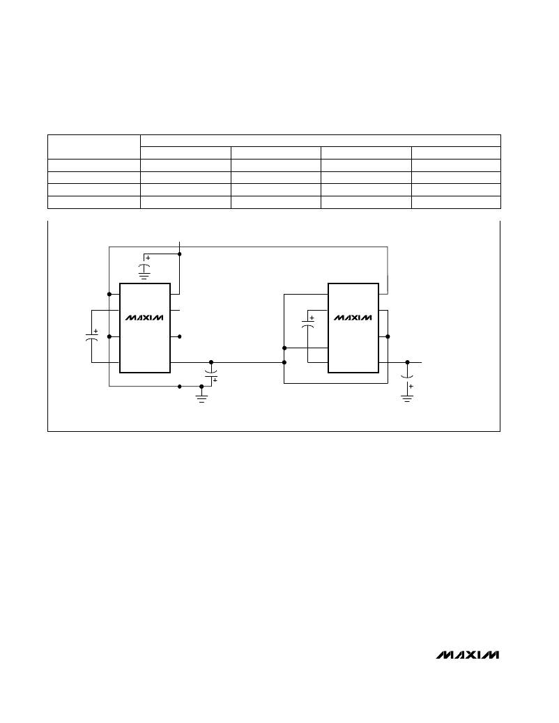
�+V� INPUT�
�1� μ� F�
�FSEL�
�CAP+�
�IN�
�SHDN�
�FSEL�
�CAP+�
�IN�
�SHDN�
�MAX1681�
�1� μ� F�
�MAX1681�
�1� μ� F�
�GND�
�LV�
�V� OUT� =� -V� INPUT�
�GND�
�LV�
�CAP-�
�OUT�
�CAP-�
�OUT�
�V� OUT� =� -2V� INPUT�
�1� μ� F�
�NOTE:� USE� 4.7� μ� F� CAPACITORS� FOR� MAX1680.�
�Figure� 1.� Cascading� MAX1680/MAX1681s� to� Increase� Output� Voltage�
�1� μ� F�
�Bypass� Capacitor�
�Bypass� the� input� voltage� to� reduce� AC� impedance� and�
�to� prevent� internal� switching� noise.� Bypassing� depends�
�on� the� source� impedance� location.� The� AC� ripple� cur-�
�rent� is� 2� x� I� OUT� for� the� doubler� and� the� inverter.� Use� a�
�large� bypass� capacitor� (equal� to� C1)� if� the� supply� has�
�high� AC� impedance.�
�Cascading� Devices�
�To� produce� larger� negative� voltages,� cascade� two�
�devices� (Figure� 1).� For� two� devices,� the� unloaded� out-�
�put� voltage� is� approximately� -2� x� V� INPUT� ,� but� this� value�
�is� reduced� slightly� by� the� first� device’s� output� resis-�
�tance� multiplied� by� the� second� device’s� quiescent� cur-�
�rent.� The� effective� output� resistance� for� a� cascaded�
�device� is� larger� than� that� for� an� individual� device� (20� ?�
�for� two� devices).� Cascading� several� devices� increases�
�output� resistance� and� reduces� efficiency.� If� a� large�
�negative� voltage� is� required� for� several� stages,� an�
�inductive� inverting� switching� regulator� such� as� the�
�MAX629� or� MAX774� may� offer� more� advantages.�
�Paralleling� Devices�
�Parallel� two� or� more� MAX1680/MAX1681s� to� reduce�
�output� resistance� voltage� drop� under� a� given� load.� With�
�reduced� output� resistance,� paralleled� devices� deliver�
�higher� load� currents.� Figure� 2� shows� two�
�MAX1680/MAX1681s� connected� in� parallel.� Output�
�resistance� is� inversely� proportional� to� the� number� of�
�devices.�
�8�
�_______________________________________________________________________________________�
�相关PDF资料 |
PDF描述 |
|---|---|
| MAX1683EUK-T | IC REG SWITCHED CAP DBL SOT23-5 |
| MAX1685EEE-T | IC REG BUCK SYNC 3.3V/ADJ 16QSOP |
| MAX1686HEUA | IC CHRG PUMP FOR SIM CARD 8-UMAX |
| MAX1688ESA+T | IC REG BOOST SYNC ADJ 2.5A 8SOIC |
| MAX16903SAUE50/V+ | IC REG BUCK SYNC 5V 1A 16TSSOP |
相关代理商/技术参数 |
参数描述 |
|---|---|
| MAX1681ESA+ | 功能描述:直流/直流开关转换器 125mA f-Select Swtcd Voltage Converter RoHS:否 制造商:STMicroelectronics 最大输入电压:4.5 V 开关频率:1.5 MHz 输出电压:4.6 V 输出电流:250 mA 输出端数量:2 最大工作温度:+ 85 C 安装风格:SMD/SMT |
| MAX1681ESA+ | 制造商:Maxim Integrated Products 功能描述:SEMICONDUCTOR ((NW)) |
| MAX1681ESA+T | 功能描述:直流/直流开关转换器 125mA f-Select Swtcd Voltage Converter RoHS:否 制造商:STMicroelectronics 最大输入电压:4.5 V 开关频率:1.5 MHz 输出电压:4.6 V 输出电流:250 mA 输出端数量:2 最大工作温度:+ 85 C 安装风格:SMD/SMT |
| MAX1681ESA-T | 功能描述:直流/直流开关转换器 125mA f-Select Swtcd Voltage Converter RoHS:否 制造商:STMicroelectronics 最大输入电压:4.5 V 开关频率:1.5 MHz 输出电压:4.6 V 输出电流:250 mA 输出端数量:2 最大工作温度:+ 85 C 安装风格:SMD/SMT |
| MAX16820ATT+ | 制造商:Maxim Integrated Products 功能描述:LED DRVR 5V/9V/12V/15V/18V/24V 6TDFN EP - Rail/Tube |
发布紧急采购,3分钟左右您将得到回复。