- 您现在的位置:买卖IC网 > PDF目录13533 > MAX1685EEE+T (Maxim Integrated Products)IC REG BUCK SYNC 3.3V/ADJ 16QSOP PDF资料下载
参数资料
| 型号: | MAX1685EEE+T |
| 厂商: | Maxim Integrated Products |
| 文件页数: | 11/14页 |
| 文件大小: | 0K |
| 描述: | IC REG BUCK SYNC 3.3V/ADJ 16QSOP |
| 产品培训模块: | Lead (SnPb) Finish for COTS Obsolescence Mitigation Program |
| 标准包装: | 2,500 |
| 类型: | 降压(降压) |
| 输出类型: | 两者兼有 |
| 输出数: | 1 |
| 输出电压: | 3.3V,1.25 V ~ 14 V |
| 输入电压: | 2.7 V ~ 14 V |
| PWM 型: | 电流模式 |
| 频率 - 开关: | 600kHz |
| 电流 - 输出: | 1A |
| 同步整流器: | 是 |
| 工作温度: | -40°C ~ 85°C |
| 安装类型: | 表面贴装 |
| 封装/外壳: | 16-SSOP(0.154",3.90mm 宽) |
| 包装: | 带卷 (TR) |
| 供应商设备封装: | 16-QSOP |
�� �
�
�Low-Noise,� 14V� Input,� 1A,� PWM�
�Step-Down� Converters�
�The� output� current� capability� for� each� mode� is� deter-�
�mined� by� the� following� equations:�
�I� OUTMAX� =� I� LIM� -� 0.5� ?� I� RIPPLE� (for� PWM� and� normal�
�modes)�
�V� OUT�
�I� OUTMAX� =� 0.5� ?� I� LIMLP� (for� low-power� mode)�
�where:�
�I� RIPPLE� =� ripple� current� =� (V� IN� -� V� OUT� )� ?� V� OUT� /� (V� IN� ?�
�f� OSC� ?� L)�
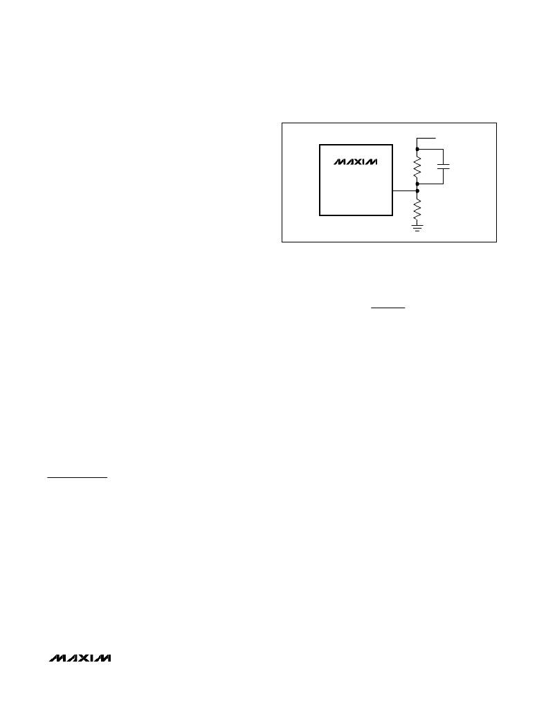
�MAX1684�
�MAX1685�
�FB�
�R1�
�R2�
�C1�
�I� LIM� =� current� limit� in� PWM� mode�
�I� LIMLP� =� current� limit� in� low-power� mode�
�Internal� Low-Voltage� Regulators� and�
�Bootstrap� (BOOT)�
�The� MAX1684/MAX1685� have� two� internal� regulators�
�(VH� and� VL)� that� generate� low-voltage� supplies� for�
�internal� circuitry� (see� the� Functional� Diagram� ).� The� VH�
�Figure� 3.� Setting� Output� Voltage�
�Connect� a� small� capacitor� across� R1� to� compensate� for�
�stray� capacitance� at� the� FB� pin:�
�regulator� generates� -4.6V� with� respect� to� IN� to� supply�
�the� P-channel� switch� and� driver.� Bypass� CVH� to� IN� with�
�a� 0.1μF� capacitor.� The� VL� regulator� generates� a� 3V� out-�
�put� at� CVL� to� supply� internal� low-voltage� blocks,� as� well�
�C1� =�
�5� (10� ?� 7� )�
�R� 2�
�as� the� N-channel� switch� and� driver.� Bypass� CVL� to�
�AGND� with� a� 1μF� capacitor.�
�To� reduce� the� quiescent� current� in� low-power� and� nor-�
�mal� modes,� connect� BOOT� to� OUT.� After� startup,� when�
�V� BOOT� exceeds� 2.6V,� the� internal� bootstrap� switch� con-�
�nects� CVL� to� BOOT.� This� bootstrap� mechanism� causes�
�the� internal� circuitry� to� be� supplied� from� the� output� and�
�thereby� reduces� the� input� quiescent� current� by� a� factor�
�of� V� OUT� /� V� IN� .� Do� not� connect� BOOT� to� OUT� if� the� out-�
�put� voltage� exceeds� 5.5V.� Instead,� connect� BOOT� to�
�AGND� to� keep� CVL� regulated� at� 3V.�
�CVL� has� a� 5mA� capability� to� supply� external� logic� cir-�
�cuitry� and� is� disabled� in� shutdown� mode.�
�Applications� Information�
�Output� Voltage� Selection�
�Connect� FB� to� AGND� to� select� the� internal� 3.3V� output�
�mode.� Connect� BOOT� to� OUT� in� this� configuration.�
�To� select� an� output� voltage� between� 1.25V� and� V� IN� ,�
�connect� FB� to� a� resistor� voltage-divider� between� the�
�output� and� AGND� (Figure� 3).� Select� R2� in� the� 20k� ?� to�
�100k� ?� range.� Calculate� R1� as� follows:�
�R1� =� R2� [(� V� OUT� /� V� FB� )� -� 1]�
�where� V� FB� =� 1.25V.�
�where:� R2� =� 100k� ?� ,� use� 4.7pF.�
�Inductor� Selection�
�The� MAX1684/MAX1685s� ’� high� switching� frequency�
�allows� the� use� of� small� surface-mount� inductors.� Table� 2�
�shows� a� selection� of� suitable� inductors� for� different� out-�
�put� voltage� ranges.� Calculate� the� minimum� inductor� by:�
�L� =� 0.9(V� OUT� -� 0.3V)� /� (I� RIPPLE� MAX� � f� OSC� )�
�where:�
�I� RIPPLE� MAX� =� should� be� less� than� or� equal� to� 400mA�
�f� OSC� =� 300kHz� (MAX1684)� or� 600kHz� (MAX1685)�
�Capacitor� Selection�
�Select� input� and� output� filter� capacitors� to� service�
�inductor� currents� while� minimizing� voltage� ripple.� The�
�input� filter� capacitor� reduces� peak� currents� and� noise�
�at� the� voltage� source.� The� MAX1684/MAX1685s’� loop�
�gain� is� relatively� low� to� enable� the� use� of� small,� low-�
�value� output� filter� capacitors.� Higher� capacitor� values�
�provide� improved� output� ripple� and� transient� response.�
�Low-ESR� capacitors� are� recommended.� Capacitor� ESR�
�is� a� major� contributor� to� output� ripple� (usually� more�
�than� 60%).� Avoid� ordinary� aluminum� electrolytic� capac-�
�itors,� as� they� typically� have� high� ESR.� Low-ESR� alu-�
�minum� electrolytic� capacitors� are� acceptable� and�
�relatively� inexpensive.� Low-ESR� tantalum� capacitors�
�are� better� and� provide� a� compact� solution� for� space-�
�constrained� surface-mount� designs.� Do� not� exceed� the�
�ripple-current� ratings� of� tantalum� capacitors.� Ceramic�
�capacitors� offer� the� lowest� ESR� overall.� Sanyo� OS-CON�
�______________________________________________________________________________________�
�11�
�相关PDF资料 |
PDF描述 |
|---|---|
| GCM43DSXS | CONN EDGECARD 86POS DIP .156 SLD |
| MAX1684EEE+T | IC REG BUCK SYNC 3.3V/ADJ 16QSOP |
| GSM24DSEF | CONN EDGECARD 48POS .156 EYELET |
| UZS1H010MCL1GB | CAP ALUM 1UF 50V 20% SMD |
| GCM43DRXS | CONN EDGECARD 86POS DIP .156 SLD |
相关代理商/技术参数 |
参数描述 |
|---|---|
| MAX1685EVKIT | 功能描述:电源管理IC开发工具 Evaluation Kit for the MAX1684 MAX1685 RoHS:否 制造商:Maxim Integrated 产品:Evaluation Kits 类型:Battery Management 工具用于评估:MAX17710GB 输入电压: 输出电压:1.8 V |
| MAX1686EUA | 功能描述:电荷泵 3-5V Regulating Chrg Pump For SIM Cards RoHS:否 制造商:Maxim Integrated 功能:Inverting, Step Up 输出电压:- 1.5 V to - 5.5 V, 3 V to 11 V 输出电流:100 mA 电源电流:1 mA 最大工作温度:+ 70 C 封装 / 箱体:SOIC-8 Narrow 封装:Tube |
| MAX1686EUA+ | 功能描述:电荷泵 3-5V Regulating Chrg Pump For SIM Cards RoHS:否 制造商:Maxim Integrated 功能:Inverting, Step Up 输出电压:- 1.5 V to - 5.5 V, 3 V to 11 V 输出电流:100 mA 电源电流:1 mA 最大工作温度:+ 70 C 封装 / 箱体:SOIC-8 Narrow 封装:Tube |
| MAX1686EUA+T | 功能描述:电荷泵 3-5V Regulating Chrg Pump For SIM Cards RoHS:否 制造商:Maxim Integrated 功能:Inverting, Step Up 输出电压:- 1.5 V to - 5.5 V, 3 V to 11 V 输出电流:100 mA 电源电流:1 mA 最大工作温度:+ 70 C 封装 / 箱体:SOIC-8 Narrow 封装:Tube |
| MAX1686EUA-T | 功能描述:电荷泵 3-5V Regulating Chrg Pump For SIM Cards RoHS:否 制造商:Maxim Integrated 功能:Inverting, Step Up 输出电压:- 1.5 V to - 5.5 V, 3 V to 11 V 输出电流:100 mA 电源电流:1 mA 最大工作温度:+ 70 C 封装 / 箱体:SOIC-8 Narrow 封装:Tube |
发布紧急采购,3分钟左右您将得到回复。