- 您现在的位置:买卖IC网 > PDF目录13549 > MAX16904SATB50/V+T (Maxim Integrated Products)IC REG BUCK SYNC 5V 0.6A 10TDFN PDF资料下载
参数资料
| 型号: | MAX16904SATB50/V+T |
| 厂商: | Maxim Integrated Products |
| 文件页数: | 3/15页 |
| 文件大小: | 0K |
| 描述: | IC REG BUCK SYNC 5V 0.6A 10TDFN |
| 产品培训模块: | Lead (SnPb) Finish for COTS Obsolescence Mitigation Program |
| 标准包装: | 2,500 |
| 类型: | 降压(降压) |
| 输出类型: | 固定 |
| 输出数: | 1 |
| 输出电压: | 5V |
| 输入电压: | 3.5 V ~ 28 V |
| PWM 型: | 电流模式 |
| 频率 - 开关: | 2.1MHz |
| 电流 - 输出: | 600mA |
| 同步整流器: | 是 |
| 工作温度: | -40°C ~ 125°C |
| 安装类型: | 表面贴装 |
| 封装/外壳: | 8-WFDFN 裸露焊盘 |
| 包装: | 带卷 (TR) |
| 供应商设备封装: | 10-TDFN-EP(3x3) |
�� �
�
�MAX16904�
�2.1MHz,� High-Voltage,�
�600mA� Mini-Buck� Converter�
�ABSOLUTE� MAXIMUM� RATINGS�
�(Voltages� referenced� to� GND.)�
�SUP,� EN..................................................................-0.3V� to� +42V�
�BST� to� LX..................................................................-0.3V� to� +6V�
�LX..............................................................-0.3V� to� (V� SUP� +� 0.3V)�
�BST� .........................................................................-0.3V� to� +47V�
�OUTS� ......................................................................-0.3V� to� +12V�
�SYNC,� PGOOD,� BIAS............................................-0.3V� to� +6.0V�
�PGND� to� GND� .......................................................-0.3V� to� +0.3V�
�LX� Continuous� RMS� Current� .................................................1.0A�
�OUTS� Short-Circuit� Duration� ......................................Continuous�
�ESD� Protection�
�Human� Body� Model� .........................................................±2kV�
�Machine� Model� ..............................................................±200V�
�Continuous� Power� Dissipation� (T� A� =� +70°C)�
�TDFN� (derate� 24.4� mW/°C� above� +70°C)......................1951mW�
�TSSOP� (derate� 26.1� mW/°C� above� +70°C)� ...................2089mW�
�Operating� Temperature� Range� .........................-40°C� to� +125°C�
�Junction� Temperature� ......................................................+150°C�
�Storage� Temperature� Range� .............................-65°C� to� +150°C�
�Lead� Temperature� (soldering,� 10s)� .................................+300°C�
�Soldering� Temperature� (reflow)� .......................................+260°C�
�Stresses� beyond� those� listed� under� “Absolute� Maximum� Ratings”� may� cause� permanent� damage� to� the� device.� These� are� stress� ratings� only,� and� functional�
�operation� of� the� device� at� these� or� any� other� conditions� beyond� those� indicated� in� the� operational� sections� of� the� specifications� is� not� implied.� Exposure� to�
�absolute� maximum� rating� conditions� for� extended� periods� may� affect� device� reliability.�
�PACKAGE� THERMAL� CHARACTERISTICS� (Note� 1)�
�TDFN�
�Junction-to-Ambient� Thermal� Resistance� (� θ� JA� )� ...........41°C/W�
�Junction-to-Case� Thermal� Resistance� (� θ� JC� )� ..................9°C/W�
�TSSOP�
�Junction-to-Ambient� Thermal� Resistance� (� θ� JA� )� ........38.3°C/W�
�Junction-to-Case� Thermal� Resistance� (� θ� JC� )� ..................3°C/W�
�Note� 1:� Package� thermal� resistances� were� obtained� using� the� method� described� in� JEDEC� specification� JESD51-7,� using� a� four-layer�
�board.� For� detailed� information� on� package� thermal� considerations,� refer� to� www.maximintegrated.com/thermal-tutorial� .�
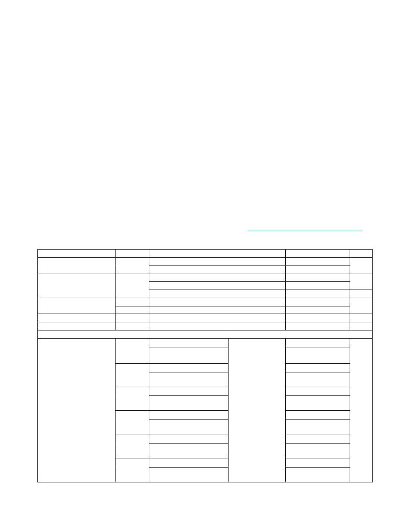
�ELECTRICAL� CHARACTERISTICS�
�(V� SUP� =� +14V,� T� A� =� T� J� =� -40°C� to� +125°C,� unless� otherwise� noted.� Typical� values� are� at� T� A� =� +25°C,� unless� otherwise� noted.)�
�PARAMETER�
�SYMBOL�
�CONDITIONS�
�MIN�
�TYP�
�MAX�
�UNITS�
�Supply� Voltage� Range�
�Supply� Current�
�V� SUP�
�I� SUP�
�(Note� 2)�
�t� <� 1s�
�EN� =� low�
�EN� =� high,� no� load,� 3V� <� V� OUT� <� 5.5V�
�3.5�
�4�
�25�
�28�
�42�
�8�
�35�
�V�
�μA�
�EN� =� high,� continuous,� no� switching�
�1�
�mA�
�UV� Lockout�
�V� UVLO�
�V� UVLO,HYS�
�Bias� rising�
�Hysteresis�
�2.8�
�3�
�0.4�
�3.2�
�V�
�Bias� Voltage�
�V� BIAS�
�+5.5V�
�V� SUP�
�+42V�
�5�
�V�
�Bias� Current� Limit�
�I� BIAS�
�10�
�mA�
�BUCK� CONVERTER�
�V� OUT� =� 5V,� fixed� frequency�
�-2.0%�
�+2.5%�
�V� OUT�
�V� OUT� =� 5V,� SKIP� mode�
�(Note� 3)�
�-2.0%�
�+4.0%�
�V� OUT� =� 5V,� fixed� frequency�
�-2.0%�
�5�
�+2.5%�
�V� OUT,5V�
�V� OUT� =� 5V,� SKIP� mode�
�(Note� 3)�
�V� OUT� =� 3.3V,� fixed� frequency�
�-2.0%�
�-2.0%�
�5�
�3.3�
�+4.0%�
�+2.5%�
�Voltage� Accuracy�
�V� OUT,3.3V�
�V� OUT,5.1V�
�V� OUT� =� 3.3V,� SKIP� mode�
�(Note� 3)�
�V� OUT� =� 5.1V,� fixed� frequency�
�V� OUT� =� 5.1V,� SKIP� mode�
�(Note� 3)�
�6V� V� SUP� 18V,�
�I� LOAD� =� 0� to� 600mA,�
�T� A� =� -40°C� to�
�+125°C�
�-2.0%�
�-2.0%�
�-2.0%�
�3.3�
�5.1�
�5.1�
�+4.0%�
�+2.5%�
�+4.0%�
�V�
�V� OUT� =� 6.0V,� fixed� frequency�
�-2.0%�
�6.0�
�+2.5%�
�V� OUT,6.0V�
�V� OUT,8.0V�
�V� OUT� =� 6.0V,� SKIP� mode�
�(Note� 3)�
�V� OUT� =� 8.0V,� fixed� frequency�
�V� OUT� =� 8.0V,� SKIP� mode�
�(Note� 3)�
�-2.0%�
�-2.0%�
�-2.0%�
�6.0�
�8.0�
�8.0�
�+4.0%�
�+2.5%�
�+4.0%�
�Maxim� Integrated�
�3�
�相关PDF资料 |
PDF描述 |
|---|---|
| VI-J4T-EX-F1 | CONVERTER MOD DC/DC 6.5V 75W |
| MAX16904SATB33/V+T | IC REG BUCK SYNC 3.3V .6A 10TDFN |
| HCM22DRKH | CONN EDGECARD 44POS DIP .156 SLD |
| MAX16904RATB50/V+T | IC REG BUCK SYNC 5V 0.6A 10TDFN |
| SCMS5D25-821 | INDUCTOR SMD 820UH 0.11A 100KHZ |
相关代理商/技术参数 |
参数描述 |
|---|---|
| MAX16904SATB51/V+T | 功能描述:直流/直流开关转换器 2.1MHz 600mA Mini Buck Converter RoHS:否 制造商:STMicroelectronics 最大输入电压:4.5 V 开关频率:1.5 MHz 输出电压:4.6 V 输出电流:250 mA 输出端数量:2 最大工作温度:+ 85 C 安装风格:SMD/SMT |
| MAX16904SATB52/V+T | 制造商:Maxim Integrated Products 功能描述:2.1MHZ, HIGH-VOLTAGE, MINI-BUCK CONVERTER - Tape and Reel 制造商:Maxim Integrated Products 功能描述:IC REG BUCK SYNC 5.2V .6A 10TDFN 制造商:Maxim Integrated Products 功能描述:Voltage Regulators - Switching Regulators |
| MAX16904SATB60/V+T | 功能描述:直流/直流开关转换器 2.1MHz, 600mA Mini Buck Converter RoHS:否 制造商:STMicroelectronics 最大输入电压:4.5 V 开关频率:1.5 MHz 输出电压:4.6 V 输出电流:250 mA 输出端数量:2 最大工作温度:+ 85 C 安装风格:SMD/SMT |
| MAX16904SATB80/V+T | 功能描述:直流/直流开关转换器 2.1MHz, 600mA Mini Buck Converter RoHS:否 制造商:STMicroelectronics 最大输入电压:4.5 V 开关频率:1.5 MHz 输出电压:4.6 V 输出电流:250 mA 输出端数量:2 最大工作温度:+ 85 C 安装风格:SMD/SMT |
| MAX16904SAUE33/V+ | 功能描述:直流/直流开关转换器 2.1MHz Mini-Buck Converter RoHS:否 制造商:STMicroelectronics 最大输入电压:4.5 V 开关频率:1.5 MHz 输出电压:4.6 V 输出电流:250 mA 输出端数量:2 最大工作温度:+ 85 C 安装风格:SMD/SMT |
发布紧急采购,3分钟左右您将得到回复。