- 您现在的位置:买卖IC网 > PDF目录16554 > MAX16922AUPF/V+ (Maxim Integrated Products)IC DCDC CONV STPDN LDO 20TSSOP PDF资料下载
参数资料
| 型号: | MAX16922AUPF/V+ |
| 厂商: | Maxim Integrated Products |
| 文件页数: | 10/17页 |
| 文件大小: | 0K |
| 描述: | IC DCDC CONV STPDN LDO 20TSSOP |
| 其它有关文件: | Automotive Product Guide |
| 产品培训模块: | Lead (SnPb) Finish for COTS Obsolescence Mitigation Program |
| 标准包装: | 74 |
| 应用: | 车载系统 |
| 电源电压: | 3.7 V ~ 28 V |
| 工作温度: | -40°C ~ 125°C |
| 安装类型: | 表面贴装 |
| 封装/外壳: | 20-TSSOP(0.173",4.40mm 宽)裸露焊盘 |
| 供应商设备封装: | 20-TSSOP-EP |
| 包装: | 管件 |
�� �
�
�MAX16922�
�2.2MHz,� Dual,� Step-Down� DC-DC�
�Converters,� Dual� LDOs,� and� RESET�
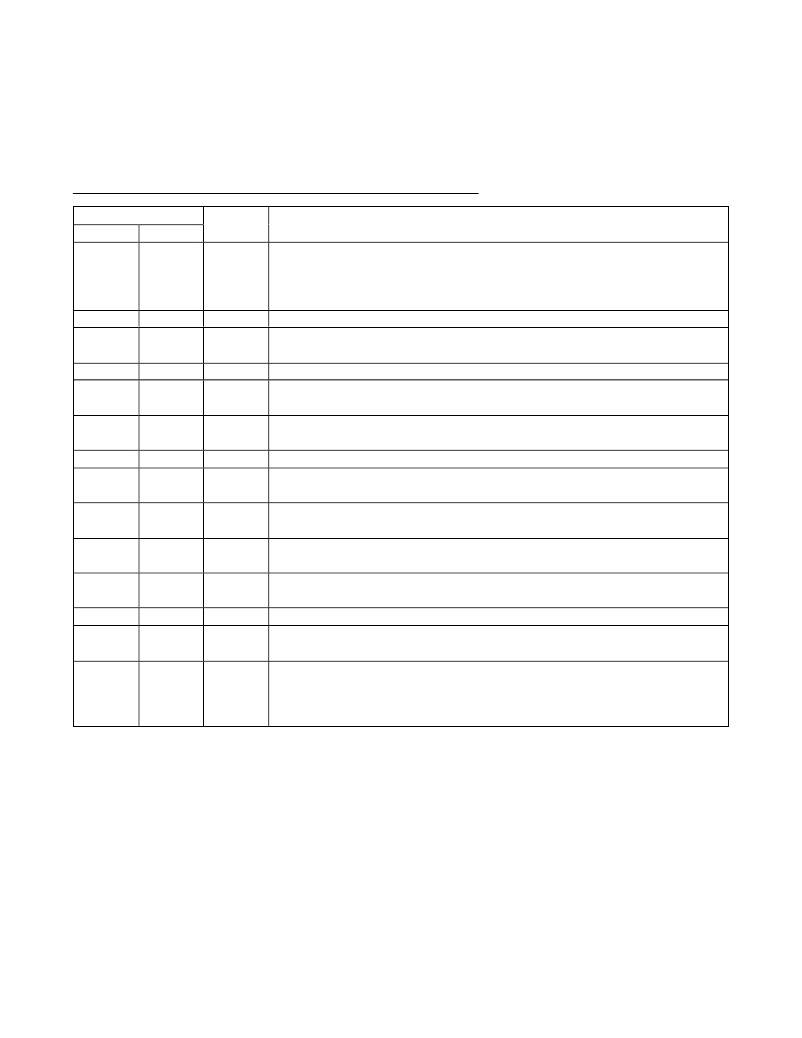
�Pin� Description� (continued)�
�TQFN�
�PIN�
�TSSOP�
�NAME�
�FUNCTION�
�OUT2� Voltage� Sense� Input.� Connect� OUTS2� directly� to� the� OUT2� output� voltage� and�
�8�
�10�
�OUTS2�
�bypass� to� PGND2� with� a� minimum� total� capacitance� of� 10μF.� The� total� capacitance� can�
�include� input� bypass� capacitors� cascaded� from� OUT2,� discharged� by� a� 70� Ω� resistance�
�between� OUTS2� and� PGND2� when� disabled.�
�9�
�10�
�11�
�12�
�13�
�14�
�15�
�16�
�17�
�18�
�19�
�20�
�11�
�12�
�13�
�14�
�15�
�16�
�17�
�18�
�19�
�20�
�1�
�2�
�PGND2�
�LX2�
�PV2�
�PV3�
�OUT3�
�GND2�
�OUT4�
�PV4�
�LSUP�
�RESET�
�GND1�
�EN�
�Power� Ground� for� BUCK� 2.� Connect� PGND2� and� GND_� together� near� the� device.�
�Inductor� Connection� for� OUT2.� Connect� a� 2.2μH� inductor� between� LX2� and� OUT2� as� shown�
�in� the� Functional� Diagram� .�
�OUT2� Supply� Input.� Connect� a� 4.7μF� or� larger� ceramic� capacitor� from� PV2� to� ground.�
�Linear-Regulator� Power� Input� for� OUT3.� Bypass� PV3� to� GND� with� a� minimum� 2.2μF� ceramic�
�capacitor.�
�Linear-Regulator� 1� Output.� Bypass� OUT3� to� GND� with� a� minimum� 2.2μF� ceramic� capacitor�
�internally� discharged� by� a� 1k� Ω� resistance� when� disabled.�
�Ground.� Connect� GND,� GND1,� GND2,� and� GND3� together.�
�Linear-Regulator� 2� Output.� Bypass� OUT4� to� GND� with� a� minimum� 2.2μF� ceramic� capacitor.�
�Internally� discharged� by� a� 1k� Ω� resistance� when� disabled.�
�Linear-Regulator� Power� Input� for� OUT4.� Bypass� PV4� to� GND� with� a� minimum� 2.2μF� ceramic�
�capacitor.�
�5V� Logic� Supply� to� Provide� Power� to� Internal� Circuitry.� Bypass� LSUP� to� GND1� with� a� 1μF�
�ceramic� capacitor.�
�Open-Drain� Reset� Output� for� the� Input� Monitoring� OUT1� and� OUT2.� External� pullup�
�required.�
�Ground.� Connect� GND,� GND1,� GND2,� and� GND3� together.�
�Active-High� Enable� Input.� Connect� EN� to� PV1� or� a� logic-high� voltage� to� turn� on� all�
�regulators.� Pull� EN� input� low� to� place� the� regulators� in� shutdown.�
�Exposed� Pad.� Connect� the� exposed� pad� to� ground.� Connecting� the� exposed� pad� to� ground�
�—�
�—�
�EP�
�does� not� remove� the� requirement� for� proper� ground� connections� to� PGND2� and� GND_.� The�
�exposed� pad� is� attached� with� epoxy� to� the� substrate� of� the� die,� making� it� an� excellent� path�
�to� remove� heat� from� the� device.�
�10�
�Maxim� Integrated�
�相关PDF资料 |
PDF描述 |
|---|---|
| HSM08DSES | CONN EDGECARD 16POS .156 EYELET |
| MAX16922AUPE/V+ | IC DCDC CONV STPDN LDO 20TSSOP |
| GCM31DCTH | CONN EDGECARD 62POS DIP .156 SLD |
| REC5-4815DRWZ/H4/C | CONV DC/DC 5W 18-72VIN +/-15VOUT |
| EBM18DCBI | CONN EDGECARD 36POS R/A .156 SLD |
相关代理商/技术参数 |
参数描述 |
|---|---|
| MAX16922AUPG/V+ | 功能描述:直流/直流开关转换器 2.2MHz Dual Step-Dwn DC/DC Converter RoHS:否 制造商:STMicroelectronics 最大输入电压:4.5 V 开关频率:1.5 MHz 输出电压:4.6 V 输出电流:250 mA 输出端数量:2 最大工作温度:+ 85 C 安装风格:SMD/SMT |
| MAX16922AUPG/V+T | 功能描述:直流/直流开关转换器 2.2MHz Dual Step-Dwn DC/DC Converter RoHS:否 制造商:STMicroelectronics 最大输入电压:4.5 V 开关频率:1.5 MHz 输出电压:4.6 V 输出电流:250 mA 输出端数量:2 最大工作温度:+ 85 C 安装风格:SMD/SMT |
| MAX16922AUPH/V+ | 功能描述:直流/直流开关转换器 2.2MHz Dual Step-Dwn DC/DC Converter RoHS:否 制造商:STMicroelectronics 最大输入电压:4.5 V 开关频率:1.5 MHz 输出电压:4.6 V 输出电流:250 mA 输出端数量:2 最大工作温度:+ 85 C 安装风格:SMD/SMT |
| MAX16922AUPH/V+T | 功能描述:直流/直流开关转换器 2.2MHz Dual Step-Dwn DC/DC Converter RoHS:否 制造商:STMicroelectronics 最大输入电压:4.5 V 开关频率:1.5 MHz 输出电压:4.6 V 输出电流:250 mA 输出端数量:2 最大工作温度:+ 85 C 安装风格:SMD/SMT |
| MAX16922EVKIT+ | 功能描述:直流/直流开关转换器 MAX16922 EVKIT RoHS:否 制造商:STMicroelectronics 最大输入电压:4.5 V 开关频率:1.5 MHz 输出电压:4.6 V 输出电流:250 mA 输出端数量:2 最大工作温度:+ 85 C 安装风格:SMD/SMT |
发布紧急采购,3分钟左右您将得到回复。