- 您现在的位置:买卖IC网 > PDF目录1227 > MAX16929EVKIT+ (Maxim Integrated Products)KIT EVALUATION FOR MAX16929 PDF资料下载
参数资料
| 型号: | MAX16929EVKIT+ |
| 厂商: | Maxim Integrated Products |
| 文件页数: | 11/25页 |
| 文件大小: | 0K |
| 描述: | KIT EVALUATION FOR MAX16929 |
| 标准包装: | 1 |
| 主要目的: | 汽车,显示器电源 |
| 嵌入式: | 否 |
| 已用 IC / 零件: | * |
| 主要属性: | 汽车,薄膜晶体管(TFT),液晶显示器(LCD)应用 |
| 已供物品: | 板 |
�� �
�
�MAX16929�
�Automotive� TFT-LCD� Power� Supply� with� Boost�
�Converter� and� Gate� Voltage� Regulators�
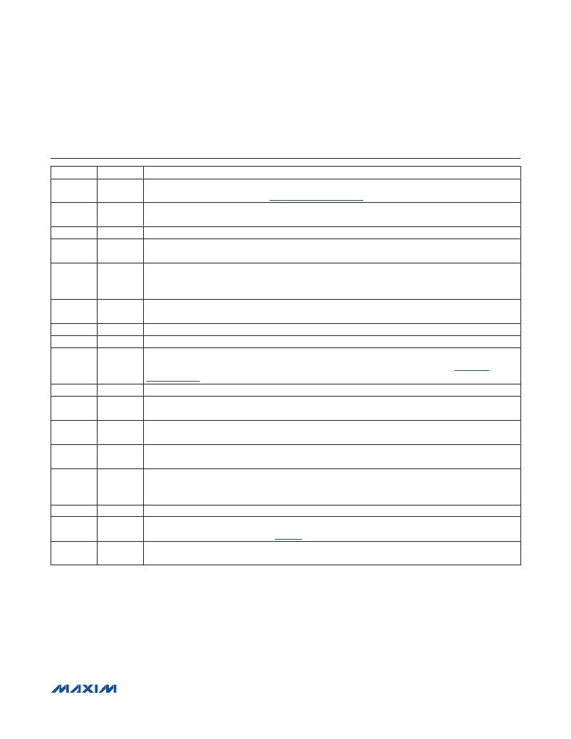
�Pin� Description� (continued)�
�PIN�
�10�
�11�
�12�
�13,� 14�
�15,� 16�
�17�
�18,� 23�
�19�
�20�
�21�
�22�
�24�
�25�
�26�
�27�
�28�
�—�
�NAME�
�FBB�
�AVL�
�BST�
�LXB�
�INB�
�ENB�
�GND�
�PGOOD�
�CP�
�GH�
�DRVN�
�COMPI�
�FBGH�
�FBGL�
�REF�
�SEQ�
�EP�
�FUNCTION�
�Buck� Converter� Feedback� Input.� FBB� is� regulated� to� either� 3.3V� or� 5V.� Connect� FBB� to� the� output-volt-�
�age� node,� OUTB,� as� shown� in� the� Typical Application Circuit� .�
�Buck� Converter� Internal� 5V� Regulator.� Connect� a� 1� F� F� capacitor� between� AVL� and� the� analog� ground�
�plane.� Do� not� use� AVL� to� power� external� circuitry.�
�Buck� Converter� Bootstrap� Capacitor� Connection.� Connect� a� 0.1� F� F� capacitor� between� BST� and� LXB.�
�Buck� Converter� Inductor� Connection.� Connect� the� inductor,� boost� capacitor,� and� catch� diode� at� this�
�node.�
�Buck� Converter� Power� Input.� Connect� to� a� 4V� to� 28V� supply.� Connect� a� 1� F� F� or� larger� ceramic� capaci-�
�tor� in� parallel� with� a� 47� F� F� bulk� capacitor� from� INB� to� the� power� ground� plane.� Connect� both� INB� power�
�inputs� together.�
�Buck� Converter� Enable� Input.� ENB� is� a� high-voltage� compatible� input.� Connect� to� INB� for� normal� opera-�
�tion� and� connect� to� ground� to� disable� the� buck� converter.�
�Analog� Ground�
�Open-Drain� Power-Good� Output.� Connect� PGOOD� to� INA� through� an� external� pullup� resistor.�
�Positive-Gate� Voltage� Regulator� Power� Input.� Connect� CP� to� the� positive� output� of� the� external� charge�
�pump.� Ensure� that� V� CP� does� not� exceed� the� CP� overvoltage� threshold� as� given� in� the� Electrical�
�Characteristics� table.�
�Positive-Gate� Voltage� Regulator� Output�
�Negative-Gate� Voltage� Regulator� Driver� Output.� DRVN� is� the� open� drain� of� an� internal� p-channel� FET.�
�Connect� DRVN� to� the� base� of� an� external� npn� pass� transistor.�
�Boost� Slope� Compensation� Connection.� Connect� a� capacitor� between� COMPI� and� GND� to� set� the�
�slope� compensation.�
�Positive-Gate� Voltage� Regulator� Feedback� Input.� FBGH� is� regulated� to� 1V.� Connect� FBGH� to� the� center�
�of� a� resistive� divider� connected� between� GH� and� GND.�
�Negative-Gate� Voltage� Regulator� Feedback� Input.� FBGL� is� regulated� to� 0.25V.� Connect� FBGL� to� the�
�center� of� a� resistive� divider� connected� between� REF� and� the� output� of� the� negative-gate� voltage�
�regulator.�
�1.25V� Reference� Output.� Bypass� REF� to� GND� with� a� 0.1� F� F� ceramic� capacitor.�
�Sequencing� Input.� SEQ� has� an� internal� 500k� I� pulldown� resistor.� SEQ� determines� the� sequence� in�
�which� V� GH� and� V� GL� power-up.� See� Table 1� for� supply� sequencing� options.�
�Exposed� Pad.� Connect� to� a� large� contiguous� copper� ground� plane� for� optimal� heat� dissipation.� Do� not�
�use� EP� as� the� only� electrical� ground� connection.�
� ????????????????????????????????????????????????????????????????� � Maxim� Integrated� Products� � � 11�
�相关PDF资料 |
PDF描述 |
|---|---|
| MAX16946EVKIT+ | KIT EVALUATION FOR MAX16946 |
| MAX17015EVKIT+ | KIT EVAL FOR MAX17015 |
| MAX17021EVKIT+ | EVAL KIT FOR MAX17021 |
| MAX1702EVKIT | EVAL KIT FOR MAX1702 |
| MAX17710EVKIT# | RD ENERGY HARVESTING |
相关代理商/技术参数 |
参数描述 |
|---|---|
| MAX16929EVKIT# | 功能描述:电源管理IC开发工具 MAX16929 Eval Kit RoHS:否 制造商:Maxim Integrated 产品:Evaluation Kits 类型:Battery Management 工具用于评估:MAX17710GB 输入电压: 输出电压:1.8 V |
| MAX16929EVKIT+ | 功能描述:电源管理IC开发工具 MAX16929 Eval Kit RoHS:否 制造商:Maxim Integrated 产品:Evaluation Kits 类型:Battery Management 工具用于评估:MAX17710GB 输入电压: 输出电压:1.8 V |
| MAX16929FGUI/V+ | 功能描述:LCD 驱动器 18V 2MHz Auto TFT-LCD Pwr Supply RoHS:否 制造商:Maxim Integrated 数位数量:4.5 片段数量:30 最大时钟频率:19 KHz 工作电源电压:3 V to 3.6 V 最大工作温度:+ 85 C 最小工作温度:- 20 C 封装 / 箱体:PDIP-40 封装:Tube |
| MAX16929FGUI/V+T | 功能描述:LCD 驱动器 18V 2MHz Auto TFT-LCD Pwr Supply RoHS:否 制造商:Maxim Integrated 数位数量:4.5 片段数量:30 最大时钟频率:19 KHz 工作电源电压:3 V to 3.6 V 最大工作温度:+ 85 C 最小工作温度:- 20 C 封装 / 箱体:PDIP-40 封装:Tube |
| MAX16929GGUI/V+ | 功能描述:LCD 驱动器 18V 2MHz Auto TFT-LCD Pwr Supply RoHS:否 制造商:Maxim Integrated 数位数量:4.5 片段数量:30 最大时钟频率:19 KHz 工作电源电压:3 V to 3.6 V 最大工作温度:+ 85 C 最小工作温度:- 20 C 封装 / 箱体:PDIP-40 封装:Tube |
发布紧急采购,3分钟左右您将得到回复。