- 您现在的位置:买卖IC网 > PDF目录383332 > MAX1703ESE (MAXIM INTEGRATED PRODUCTS INC) 1-Cell to 3-Cell, High-Power 1.5A, Low-Noise, Step-Up DC-DC Converter PDF资料下载
参数资料
| 型号: | MAX1703ESE |
| 厂商: | MAXIM INTEGRATED PRODUCTS INC |
| 元件分类: | 稳压器 |
| 英文描述: | 1-Cell to 3-Cell, High-Power 1.5A, Low-Noise, Step-Up DC-DC Converter |
| 中文描述: | SWITCHING REGULATOR, 340 kHz SWITCHING FREQ-MAX, PDSO16 |
| 封装: | 0.150 INCH, SOIC-16 |
| 文件页数: | 13/16页 |
| 文件大小: | 273K |
| 代理商: | MAX1703ESE |
Bypass Capacitors
A few ceramic bypass capacitors are required for proper
operation. Bypass REF with a 0.22μF capacitor to GND.
Connect a 0.22μF ceramic capacitor from OUT to GND.
Each of these should be placed as close to their respec-
tive pins as possible, within 0.2in. (5mm) of the DC-DC
converter IC. See Table 4 for suggested suppliers.
__________ Applications Information
Intermittent Supply/Battery Connections
When boosting an input supply connected via a
mechanical switch, or a battery connected via spring
contacts, input power may sometimes be intermittent
as a result of contact bounce. When operating in PFM
mode with input voltages greater than 2.5V, restarting
after such dropouts may initiate high current pulses that
interfere with the MAX1703’s internal MOSFET switch
control. If contact or switch bounce is anticipated in the
design, use one of the following solutions:
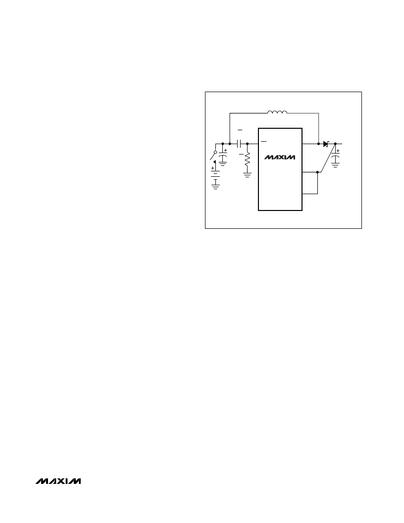
1) Connect a capacitor (C
ON
) from
ON
to V
IN
and a
1M
resistor (R
ON
) from
ON
to GND, as shown in
Figure 7. This resistor-capacitor network differenti-
ates fast input edges at V
IN
and momentarily holds
the IC off until V
IN
settles. The appropriate value of
C
ON
is 10
-5
times the total output filter capacitance
(C
OUT
), so a C
OUT
of 440μF results in C
ON
= 4.7nF.
2) Use the system microcontroller to hold the MAX1703
in shutdown from the time when power is applied (or
reapplied) until C
OUT
has charged to at least the
input voltage. Standard power-on-reset times
accomplish this.
3) Ensure that the IC operates, or at least powers up, in
PWM mode (CLK/SEL = high). Activate PFM mode
only after the output voltage has settled and all of
the system’s power-on-reset flags are cleared.
Use in a Typical Wireless
Phone Application
The MAX1703 is ideal for use in digital cordless and
PCS phones. The power amplifier (PA) is connected
directly to the boost-converter output for maximum volt-
age swing (Figure 8). Low-dropout linear regulators are
used for post-regulation to generate low-noise power
for DSP, control, and RF circuitry. Typically, RF phones
spend most of their life in standby mode with only short
periods in transmit/receive mode. During standby, max-
imize battery life by setting CLK/SEL = 0; this places
the IC in low-power mode (for the lowest quiescent
power consumption). See Gain Block section for infor-
mation on configuring an external MOSFET as a linear
regulator.
Designing a PC Board
High switching frequencies and large peak currents
make PC board layout an important part of design.
Poor design can cause excessive EMI and ground
bounce, both of which can cause instability or regula-
tion errors by corrupting the voltage and current feed-
back signals.
Power components—such as the inductor, converter
IC, filter capacitors, and output diode—should be
placed as close together as possible, and their traces
should be kept short, direct, and wide. A separate low-
noise ground plane containing the reference and signal
grounds should only connect to the power-ground
plane at one point. This minimizes the effect of power-
ground currents on the part.
Keep the voltage feedback network very close to the
IC, within 0.2in. (5mm) of the FB pins. Keep noisy
traces, such as from the LX pin, away from the voltage
feedback networks and separated from them using
grounded copper. Consult the MAX1703 EV kit for a full
PC board example.
Soft-Start
To implement soft-start, set CLK/SEL low on power-up;
this forces PFM operation and reduces the peak
switching current to 800mA max. Once the circuit is in
regulation and start-up transients have settled,
CLK/SEL can be set high for full-power operation.
M
1-Cell to 3-Cell, High-Power (1.5A),
Low-Noise, Step-Up DC-DC Converter
______________________________________________________________________________________
13
OUT
POUT
LXP, LXN
C
2 x 220
μ
F
11, 14
16
4
15, 13
C
4.7nF
R
ON
1M
ON
MAX1703
Figure 7. Connecting C
ON
and R
ON
when Switch or Battery-
Contact Bounce is Anticipated
相关PDF资料 |
PDF描述 |
|---|---|
| MAX1705 | 1- to 3-Cell, High-Current, Low-Noise, Step-Up DC-DC Converters with Linear Regulator |
| MAX1706C | 1- to 3-Cell, High-Current, Low-Noise, Step-Up DC-DC Converters with Linear Regulator |
| MAX1706D | BALUN HYBRID 750-950MHZ 1:4 |
| MAX1705C | 1- to 3-Cell, High-Current, Low-Noise, Step-Up DC-DC Converters with Linear Regulator |
| MAX1705D | 1- to 3-Cell, High-Current, Low-Noise, Step-Up DC-DC Converters with Linear Regulator |
相关代理商/技术参数 |
参数描述 |
|---|---|
| MAX1703ESE+ | 功能描述:直流/直流开关转换器 1-3 Cell 1A Step-Up DC/DC Converters RoHS:否 制造商:STMicroelectronics 最大输入电压:4.5 V 开关频率:1.5 MHz 输出电压:4.6 V 输出电流:250 mA 输出端数量:2 最大工作温度:+ 85 C 安装风格:SMD/SMT |
| MAX1703ESE+T | 功能描述:直流/直流开关转换器 1-3 Cell 1A Step-Up DC/DC Converters RoHS:否 制造商:STMicroelectronics 最大输入电压:4.5 V 开关频率:1.5 MHz 输出电压:4.6 V 输出电流:250 mA 输出端数量:2 最大工作温度:+ 85 C 安装风格:SMD/SMT |
| MAX1703ESE-T | 功能描述:直流/直流开关转换器 1-3 Cell 1A Step-Up DC/DC Converters RoHS:否 制造商:STMicroelectronics 最大输入电压:4.5 V 开关频率:1.5 MHz 输出电压:4.6 V 输出电流:250 mA 输出端数量:2 最大工作温度:+ 85 C 安装风格:SMD/SMT |
| MAX1703EVKIT | 功能描述:直流/直流开关转换器 Evaluation Kit for the MAX1703 RoHS:否 制造商:STMicroelectronics 最大输入电压:4.5 V 开关频率:1.5 MHz 输出电压:4.6 V 输出电流:250 mA 输出端数量:2 最大工作温度:+ 85 C 安装风格:SMD/SMT |
| MAX17040EVKIT+ | 制造商:Maxim Integrated Products 功能描述:MAX17040G+ EVAL KIT - Boxed Product (Development Kits) |
发布紧急采购,3分钟左右您将得到回复。