- 您现在的位置:买卖IC网 > PDF目录383332 > MAX1705C (Maxim Integrated Products, Inc.) 1- to 3-Cell, High-Current, Low-Noise, Step-Up DC-DC Converters with Linear Regulator PDF资料下载
参数资料
| 型号: | MAX1705C |
| 厂商: | Maxim Integrated Products, Inc. |
| 元件分类: | DC/DC变换器 |
| 英文描述: | 1- to 3-Cell, High-Current, Low-Noise, Step-Up DC-DC Converters with Linear Regulator |
| 中文描述: | 1 - 3节电池,大电流,低噪声,升压型DC - DC转换器与线性稳压器 |
| 文件页数: | 16/20页 |
| 文件大小: | 215K |
| 代理商: | MAX1705C |
M
1- to 3-Cell, High-Current, Low-Noise,
Step-Up DC-DC Converters with Linear Regulator
16
______________________________________________________________________________________
from higher-impedance batteries, consider using one
or two 100μF, 100m
, low-ESR tantalum capacitors.
Low-ESR capacitors are recommended. Capacitor ESR
is a major contributor to output ripple—often more than
70%.
Ceramic, Sanyo OS-CON, and Panasonic SP/CB-series
capacitors offer the lowest ESR. Low-ESR tantalum
capacitors are second best and generally offer a good
trade-off between price and performance. Do not
exceed the ripple-current ratings of tantalum capaci-
tors. Avoid aluminum-electrolytic capacitors, since their
ESR is too high.
Adding Bypass Capac itors
Several ceramic bypass capacitors are required for
proper operation of the MAX1705/MAX1706. Bypass
REF with a 0.33μF capacitor to GND. Connect a 0.1μF
ceramic capacitor from OUT to GND and a 0.33μF
ceramic capacitor from POUT to PGND. Place a 22μF,
low-ESR capacitor and an optional 0.33μF ceramic
capacitor from the linear-regulator output LDO to GND.
An optional 22pF ceramic capacitor can be added to
the linear-regulator feedback network to reduce noise
(C2, Figure 2). Place each of these as close to their
respective pins as possible, within 0.2in. (5mm) of the
DC-DC converter IC. High-value, low-voltage, surface-
mount ceramic capacitors are now readily available in
small packages; see Table 4 for suggested suppliers.
Designing a PC Board
High switching frequencies and large peak currents
make PC board layout an important part of design.
Poor design can cause excessive EMI and ground-
bounce, both of which can cause instability or
regulation errors by corrupting voltage- and current-
feedback signals. It is highly recommended that the PC
board example of the MAX1705 evaluation kit (EV kit)
be followed.
Power components—such as the inductor, converter
IC, filter capacitors, and output diode—should be
placed as close together as possible, and their traces
should be kept short, direct, and wide. Place the LDO
output capacitor as close to the LDO pin as possible.
Make the connection between POUT and OUT very
short. Keep the extra copper on the board, and inte-
grate it into ground as a pseudo-ground plane.
On multilayer boards, do not connect the ground pins
of the power components using vias through an internal
ground plane. Instead, place them close together and
route them in a star-ground configuration using compo-
nent-side copper. Then connect the star ground to the
internal ground plane using vias.
Keep the voltage-feedback networks very close to the
MAX1705/MAX1706—within 0.2in. (5mm) of the FB and
FBLDO pins. Keep noisy traces, such as from the LX
pin, away from the reference and voltage-feedback net-
works, especially the LDO feedback, and separated
from them using grounded copper. C onsult the
MAX1705/MAX1706 EV kit for a full PC board example.
__________ Applic ations Information
Use in a T ypic al
Wireless Phone Applic ation
The MAX1705/MAX1706 are ideal for use in digital cord-
less and PCS phones. The power amplifier (PA) is con-
nected directly to the step-up converter output for
maximum voltage swing (Figure 9). The internal linear
regulator is used for post-regulation to generate low-
noise power for DSP, control, and RF circuitry. Typically,
RF phones spend most of their life in standby mode and
short periods in transmit/receive mode. During standby,
maximize battery life by setting CLK/SEL = GND and
TRACK = OUT; this places the IC in PFM and track
modes (for lowest quiescent power consumption). In
transmit/receive mode, set TRACK = GND and CLK/SEL
= OUT to increase the PA supply voltage and initiate
high-power, low-noise PWM operation. Table 5 lists the
typical available output current when operating with
one or more NiCd/NiMH cells or one Li-Ion cell.
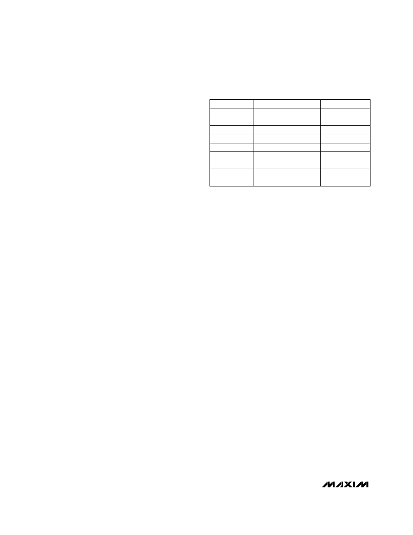
Table 4. Component Suppliers
(847) 956-0702
81-3-3607-5144
USA: (847) 956-0666
J apan: 81-3-3607-5111
Sumida
(619) 661-1055
81-7-2070-1174
USA: (619) 661-6835
J apan: 81-7-2070-6306
Sanyo
(602) 994-6430
USA: (602) 303-5454
Motorola
(714) 960-6492
USA: (714) 969-2491
Matsuo
(847) 639-1469
USA: (847) 639-6400
Coilcraft
(803) 626-3123
USA: (803) 946-0690
(800) 282-4975
AVX
FAX
PHONE
SUPPLIER
相关PDF资料 |
PDF描述 |
|---|---|
| MAX1705D | 1- to 3-Cell, High-Current, Low-Noise, Step-Up DC-DC Converters with Linear Regulator |
| MAX1705EEE | 18-Bit Universal Bus Transceivers With 3-State Outputs 56-SSOP -40 to 85 |
| MAX1706 | 1- to 3-Cell, High-Current, Low-Noise, Step-Up DC-DC Converters with Linear Regulator |
| MAX1706EEE | 1- to 3-Cell, High-Current, Low-Noise, Step-Up DC-DC Converters with Linear Regulator |
| MAX1708 | High-Frequency, High-Power, Low-Noise, Step-Up DC-DC Converter |
相关代理商/技术参数 |
参数描述 |
|---|---|
| MAX1705EEE | 功能描述:直流/直流开关转换器 1-3 Cell Step-Up w/Linear Regulator RoHS:否 制造商:STMicroelectronics 最大输入电压:4.5 V 开关频率:1.5 MHz 输出电压:4.6 V 输出电流:250 mA 输出端数量:2 最大工作温度:+ 85 C 安装风格:SMD/SMT |
| MAX1705EEE+ | 功能描述:直流/直流开关转换器 1-3 Cell Step-Up w/Linear Regulator RoHS:否 制造商:STMicroelectronics 最大输入电压:4.5 V 开关频率:1.5 MHz 输出电压:4.6 V 输出电流:250 mA 输出端数量:2 最大工作温度:+ 85 C 安装风格:SMD/SMT |
| MAX1705EEE+T | 功能描述:直流/直流开关转换器 1-3 Cell Step-Up w/Linear Regulator RoHS:否 制造商:STMicroelectronics 最大输入电压:4.5 V 开关频率:1.5 MHz 输出电压:4.6 V 输出电流:250 mA 输出端数量:2 最大工作温度:+ 85 C 安装风格:SMD/SMT |
| MAX1705EEE-T | 功能描述:直流/直流开关转换器 1-3 Cell Step-Up w/Linear Regulator RoHS:否 制造商:STMicroelectronics 最大输入电压:4.5 V 开关频率:1.5 MHz 输出电压:4.6 V 输出电流:250 mA 输出端数量:2 最大工作温度:+ 85 C 安装风格:SMD/SMT |
| MAX1705ESE+ | 制造商:Maxim Integrated Products 功能描述:1 TO 3-CELL HIGH-CURRENT LOW-NOIS - Rail/Tube |
发布紧急采购,3分钟左右您将得到回复。